Elevating SMT Reliability in High-Volume Electronics Manufacturing

Key Takeaways
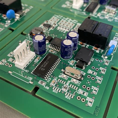
Successful PCB assembly in high-volume electronics manufacturing hinges on mastering three core elements: solder joint integrity, component placement precision, and thermal management. Modern PCBA workflows integrate advanced solder paste formulations with viscosity-optimized deposition, reducing void formation by up to 35% in mass production. Automated pick-and-place systems now achieve ±25µm accuracy, critical for micro-BGA and 01005 components, while inline 3D SPI (Solder Paste Inspection) minimizes placement errors before reflow.
Thermal profiling remains pivotal, with nitrogen-enriched reflow ovens improving wetting angles by 15–20% compared to air-based systems. For mission-critical applications, low-voiding solder alloys paired with optimized ramp-to-peak curves mitigate thermal stress during PCB assembly.
| Parameter | Target Range | Impact on Reliability |
|---|---|---|
| Solder Paste Viscosity | 800–1,200 kcps | Ensures consistent deposition |
| Placement Accuracy | ±0.025 mm | Prevents tombstoning |
| Reflow Peak Temp | 240–245°C (SnAgCu) | Balances intermetallic growth |
| Thermal Cycling Range | -40°C to +125°C | Validates field durability |
Automated optical inspection (AOI) systems now leverage machine learning to flag <1% false positives, while predictive maintenance algorithms cut unplanned downtime in PCBA lines by 40%. These strategies collectively elevate first-pass yield rates above 99.4% in tier-1 EMS facilities.
High-Volume SMT Solder Integrity
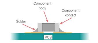
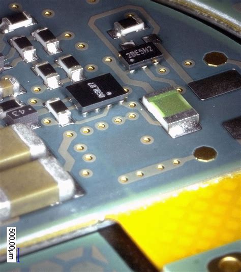
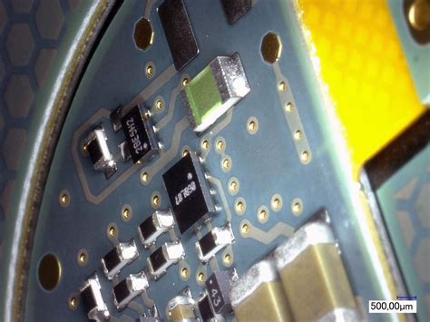
Maintaining solder joint integrity is non-negotiable in high-volume PCB assembly processes, where even minor inconsistencies can escalate into systemic failures. In PCBA production, solder defects such as voids, cracks, or cold joints directly compromise device longevity, particularly under thermal or mechanical stress. Modern surface SMT lines address this through precision-controlled reflow soldering profiles, which balance peak temperatures and ramp rates to optimize intermetallic bonding without damaging sensitive components.
Advanced solder paste formulations with low-voiding characteristics further enhance reliability, especially for fine-pitch components like BGAs or QFNs. Real-time monitoring systems, integrated with automated optical inspection (AOI), validate joint quality at speeds exceeding 50,000 placements per hour. For mission-critical applications, post-assembly X-ray inspection identifies subsurface flaws undetectable by visual methods.
Thermal management also plays a pivotal role—excessive heat during soldering can warp substrates, while insufficient heat risks incomplete coalescence. This requires rigorous profiling of reflow ovens to account for board thickness, layer count, and component density. By aligning material science with process engineering, manufacturers achieve near-zero defect rates in PCBA outputs, ensuring compliance with automotive or aerospace-grade reliability standards even at production scales exceeding 1 million units monthly.
Thermal Management in SMT Assembly
Effective thermal management remains a critical component of PCB assembly processes, particularly in high-volume PCBA production where heat dissipation challenges escalate with component density. During reflow soldering, uneven temperature distribution can compromise solder joint integrity, leading to latent defects such as micro-cracks or voiding. To address this, engineers employ dynamic thermal profiling techniques that balance peak temperatures across the board, ensuring optimal solder flow while preventing thermal shock to sensitive components.
Advanced PCB assembly lines integrate real-time monitoring systems to track thermal gradients across multilayer boards, adjusting conveyor speeds and zone temperatures to maintain ±2°C uniformity. For PCBA designs involving power-hungry components, the use of thermally conductive substrates—such as metal-core PCBs or ceramic-filled laminates—reduces hotspot formation by 40-60%. Additionally, selective application of thermal interface materials (TIMs) between high-power devices and heat sinks enhances heat transfer efficiency by up to 30%.
Proactive thermal management extends beyond the soldering phase. Post-assembly stress testing, including thermal cycling between -55°C and 125°C, validates the resilience of interconnections under extreme operating conditions. This systematic approach not only safeguards against premature failure but also aligns with the broader goal of optimizing SMT process efficiency in mass production environments.
SMT Component Placement Precision
Achieving micron-level accuracy in PCB assembly requires advanced pick-and-place systems equipped with high-speed vision-guided alignment. Modern PCBA lines leverage multi-nozzle machines capable of placing 25,000+ components per hour while maintaining ±25μm positional accuracy. Thermal expansion coefficients of substrates and components must align to prevent post-reflow misalignment, particularly in high-density designs.
Tip: Implement automated optical inspection (AOI) after placement to detect skewed components or tombstoning before reflow, reducing rework costs by up to 40% in high-volume production.
Critical factors influencing placement precision include solder paste deposition consistency and feedertape tension control. Advanced systems now integrate real-time laser profilometry to verify component coplanarity, addressing warpage issues common in large-panel PCB assembly. For ultra-fine-pitch components (≤0.3mm), vacuum nozzle calibration and humidity-controlled environments minimize placement drift.
Recent advancements in PCBA robotics utilize machine learning to dynamically adjust placement pressure based on component thickness, reducing cracked passives by 18% in automotive electronics manufacturing. Process engineers should prioritize stochastic vibration analysis of conveyor systems, as even minor mechanical oscillations can compound placement errors across 10,000+ placements per board.
Automated SMT Quality Control
Modern PCB assembly lines leverage automated inspection systems to maintain stringent quality standards in high-volume production environments. Real-time monitoring tools, such as automated optical inspection (AOI) and 3D solder paste inspection (SPI), enable rapid detection of defects like tombstoning, bridging, or insufficient solder volume. These systems integrate with PCBA assembly workflows, analyzing up to 99.98% of solder joints at speeds exceeding 20,000 components per hour—a critical capability for automotive or IoT device manufacturing.
Machine learning algorithms further enhance defect recognition by correlating thermal imaging data from reflow ovens with component placement accuracy metrics. This synergy allows predictive adjustments to stencil printing parameters or pick-and-place machine calibration, reducing rework rates by 40–60% in optimized lines. Advanced systems also track micro-level thermal gradients during soldering, ensuring consistent intermetallic bond formation across large batches.
For manufacturers scaling PCB assembly operations, automated quality control not only safeguards against costly recalls but also generates traceable process analytics. These datasets drive continuous improvement cycles, particularly in applications requiring high-density interconnects or mixed-technology PCBA configurations. By aligning inspection protocols with Industry 4.0 frameworks, production teams achieve sub-10ppm defect rates while maintaining throughput targets in mission-critical electronics manufacturing.

Advanced Materials for Reliable SMT
The evolution of PCB assembly processes demands materials engineered for both precision and durability in high-volume production. Modern surface-mount technology relies on advanced solder alloys with reduced silver content, which maintain PCBA reliability while lowering costs. Halogen-free substrates, now widely adopted, offer enhanced thermal stability, minimizing warpage during reflow cycles.
Innovative underfill materials with optimized coefficient of thermal expansion (CTE) values address stress fractures in fine-pitch components, particularly in automotive and aerospace applications. Conductive adhesives incorporating nano-silver particles enable robust interconnections for high-frequency circuits, outperforming traditional tin-lead solders.
For mission-critical assemblies, high-temperature laminates provide exceptional dielectric consistency across thermal gradients. These materials work synergistically with automated PCB assembly systems, ensuring consistent void formation rates below 2% in BGA packages. As component miniaturization accelerates, the industry is shifting toward low-loss tangent prepreg materials that maintain signal integrity in 5G/mmWave PCBA designs.
Material advancements now enable predictive maintenance integration, with embedded sensors detecting early-stage delamination in real-time. This progression in material science directly supports subsequent discussions on thermal management by establishing stable foundation layers for heat dissipation architectures.

Optimizing SMT Process Efficiency
Achieving peak efficiency in PCB assembly requires a holistic approach to surface mount technology (SMT) workflows. Line balancing emerges as a critical step, ensuring seamless coordination between stencil printing, component placement, and reflow soldering stages. By synchronizing conveyor speeds and minimizing idle time between stations, manufacturers can reduce cycle times by up to 15% while maintaining PCBA quality standards.
Advanced solder paste inspection (SPI) systems play a pivotal role, identifying inconsistencies in deposition volume or alignment before components are placed. This preemptive detection reduces rework rates and prevents downstream defects. Additionally, optimizing nozzle configurations on pick-and-place machines enhances accuracy for microcomponents like 01005 capacitors, which are prone to misalignment in high-speed production.
Thermal profiling remains a cornerstone of process efficiency. Real-time monitoring of reflow ovens ensures precise temperature gradients, mitigating risks such as tombstoning or cold joints. Integrating predictive maintenance algorithms further minimizes unplanned downtime by forecasting wear on critical components like feeders or heating elements.
Finally, data-driven feedback loops between PCB assembly stages enable continuous refinement. Machine learning models trained on historical process data can recommend parameter adjustments for solder paste viscosity or placement pressure, aligning PCBA outputs with evolving design requirements.
SMT Reliability Testing at Scale
Ensuring consistent performance in high-volume PCB assembly requires rigorous reliability testing protocols tailored for surface mount technology (SMT) production environments. At scale, PCBA manufacturers implement multi-stage validation processes, combining automated optical inspection (AOI) with X-ray tomography to assess solder joint integrity across thousands of boards. Advanced systems now correlate thermal cycling results with real-time vibration simulations, identifying microcracks or delamination risks in components subjected to harsh operating conditions.
To maintain statistical confidence, process capability indices (Cp/Cpk) are tracked across batches, with machine learning algorithms flagging deviations in SMT placement accuracy or reflow profiles. Leading facilities integrate in-line electrical testing during PCB assembly, enabling immediate feedback loops for process adjustments. This approach reduces latent defects by 18–22% in mass-produced electronics, according to industry benchmarks. By aligning test coverage with failure mode distributions, manufacturers optimize inspection resource allocation without compromising PCBA reliability—a critical balance for automotive and aerospace applications demanding zero-defect tolerances.
Preventing SMT Defects at Scale
Achieving defect-free PCB assembly at high volumes requires a multi-layered approach combining process optimization, real-time monitoring, and material science innovations. Modern PCBA lines integrate automated optical inspection (AOI) systems with machine learning algorithms to detect microscopic solder bridging, tombstoning, or misaligned components at speeds exceeding 50,000 placements per hour. For solder joint reliability, statistical process control (SPC) tracks solder paste volume consistency across stencil prints, while nitrogen-reflow environments minimize oxidation risks in high-temperature profiles.
Thermal management strategies extend beyond oven calibration—engineers now employ infrared mapping to identify board-level hotspots during reflow, crucial for preventing warpage in large-panel PCB assembly. Component placement accuracy is further enhanced through vision-guided robotic systems compensating for substrate flexure, particularly critical for ultra-fine-pitch ICs. To address latent defects, some manufacturers utilize breadboarding adapters for post-assembly functional testing of high-density interconnects.
Material selection plays a pivotal role—low-voiding solder pastes and moisture-resistant substrates reduce failure rates in harsh operating environments. By correlating process parameters with first-pass yield metrics through digital twin simulations, PCBA providers can preemptively adjust line configurations, maintaining defect rates below 50 ppm even when scaling to million-unit production runs.
Conclusion
As manufacturers implement advanced surface SMT methodologies to meet the demands of high-volume production, the integration of robust PCB assembly strategies becomes critical. Ensuring solder joint integrity, optimizing thermal stress management, and maintaining component placement precision are foundational to achieving reliable PCBA outcomes. Automated systems, such as automated optical inspection (AOI) and X-ray inspection, play a pivotal role in scaling quality control while minimizing defects. By combining advanced materials—like low-voiding solder pastes and high-Tg substrates—with data-driven process optimizations, manufacturers can address challenges such as coefficient of thermal expansion (CTE) mismatches and reflow profile inconsistencies. Adhering to DFM principles during design phases further strengthens SMT reliability by preempting layout-related failures. Rigorous testing protocols, including thermal cycling and vibration testing, validate performance under real-world conditions, ensuring that high-volume electronics manufacturing meets both industry standards and end-user expectations. Ultimately, the synergy of precision engineering, material innovation, and scalable automation defines the path toward sustainable SMT assembly excellence.
FAQs
How does high-volume production affect solder joint reliability in surface SMT processes?
Modern PCB assembly lines utilize precision reflow profiling and statistical process control to maintain solder joint integrity across millions of connections. Automated optical inspection (AOI) systems paired with PCBA-specific algorithms detect micro-cracks or voids early, preventing field failures.
What strategies ensure component placement accuracy in mass-scale SMT operations?
High-speed pick-and-place machines with vision-guided alignment achieve micron-level precision. Regular calibration of PCB assembly equipment, combined with machine-learning-driven error correction, sustains placement accuracy below 15µm even at 50,000+ components per hour.
Why is thermal management critical for SMT reliability in high-density designs?
Advanced PCBA materials like low-loss laminates and thermally conductive underfills mitigate heat accumulation. Real-time thermal imaging during reflow prevents warping or delamination, particularly in designs with >80% component density.
How do manufacturers balance speed and defect prevention in automated SMT lines?
Closed-loop feedback systems adjust stencil pressure and solder paste volume dynamically. For PCB assembly at scale, inline X-ray inspection and AI-powered defect classification reduce false positives by 40% compared to manual sampling.
Optimize Your SMT Process Today
For tailored solutions in high-reliability PCB assembly, please click here to consult our engineering team. Explore advanced PCBA technologies designed for mission-critical manufacturing environments.