Embedded Component PCB Technology: Design, Manufacturing, and Applications
Abstract
Embedded component PCB (Printed Circuit Board) technology represents a significant advancement in electronic packaging, offering improved performance, reduced size, and enhanced reliability. This paper explores the fundamental principles, manufacturing processes, materials, design considerations, and applications of embedded component PCB technology. By integrating passive and active components within the PCB substrate, this technology enables higher-density interconnects, better signal integrity, and improved thermal management. The discussion covers various embedding techniques, challenges in implementation, and future trends in the industry.
1. Introduction
The demand for compact, high-performance electronic devices has driven innovations in PCB technology. Traditional surface-mounted components occupy valuable board space and can limit design flexibility. Embedded component PCB technology addresses these challenges by incorporating components such as resistors, capacitors, inductors, and even ICs within the layers of the PCB substrate.
This approach offers several advantages:
- Miniaturization: Reduced footprint by eliminating surface-mounted parts.
- Improved Electrical Performance: Shorter interconnects reduce parasitic effects.
- Enhanced Reliability: Protection from mechanical stress and environmental factors.
- Better Thermal Management: Heat dissipation through the substrate.
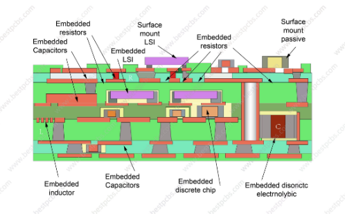
2. Types of Embedded Components
Embedded components can be classified into two main categories:
2.1 Passive Embedded Components
Passive components such as resistors, capacitors, and inductors are commonly embedded using thin-film or thick-film technologies.
- Embedded Resistors: Fabricated using resistive materials like NiP or carbon-based pastes.
- Embedded Capacitors: Created using high-dielectric-constant materials (e.g., barium titanate).
- Embedded Inductors: Formed by spiral conductive traces within the PCB layers.
2.2 Active Embedded Components
Active components, including ICs and bare dies, can also be embedded using advanced techniques like:
- Chip-in-PCB: Dies are placed in cavities and interconnected via microvias.
- Fan-Out Wafer-Level Packaging (FO-WLP): Dies are embedded in a mold compound and redistributed.
3. Manufacturing Processes
The fabrication of embedded component PCBs involves several key steps:
3.1 Substrate Preparation
- Core Material Selection: High-Tg FR4, polyimide, or ceramic-based materials.
- Laser Drilling & Cavity Formation: Precision cavities are created for component placement.
3.2 Component Integration
- Thin-Film Deposition: Sputtering or electroplating for embedded passives.
- Pick-and-Place for Active Dies: High-accuracy placement systems ensure proper alignment.
3.3 Lamination & Interconnection
- Resin Coating & Lamination: Components are encapsulated under high pressure and temperature.
- Laser Direct Structuring (LDS): Microvias and interconnects are formed.
3.4 Final Processing
- Surface Finishing: ENIG (Electroless Nickel Immersion Gold) or OSP (Organic Solderability Preservative).
- Testing & Inspection: Electrical testing and X-ray inspection ensure reliability.
4. Design Considerations
Designing embedded component PCBs requires careful planning:
4.1 Signal Integrity & EMI Control
- Controlled Impedance Routing: Minimizes signal reflections.
- Shielding Techniques: Embedded ground planes reduce electromagnetic interference.
4.2 Thermal Management
- Thermal Vias & Heat Spreaders: Dissipate heat from embedded ICs.
- Material Selection: High-thermal-conductivity dielectrics improve heat transfer.
4.3 Reliability & Testing
- Stress Analysis: Ensures mechanical stability under thermal cycling.
- Accelerated Life Testing: Validates long-term performance.
5. Applications
Embedded component PCBs are used in various industries:
- Consumer Electronics: Smartphones, wearables, and IoT devices.
- Automotive: ADAS (Advanced Driver Assistance Systems), infotainment.
- Aerospace & Defense: Avionics, radar systems.
- Medical Devices: Implantable electronics, diagnostic equipment.
6. Challenges & Future Trends
Despite its advantages, embedded component PCB technology faces challenges:
- Higher Manufacturing Costs: Complex processes increase production expenses.
- Rework Difficulty: Repairing embedded components is challenging.
- Standardization Issues: Lack of uniform industry standards.
Future trends include:
- 3D Printed Embedded Electronics: Additive manufacturing for rapid prototyping.
- Advanced Materials: Nanocomposites for better performance.
- AI-Assisted Design: Machine learning optimizes component placement.
7. Conclusion
Embedded component PCB technology is revolutionizing electronics by enabling smaller, faster, and more reliable devices. While challenges remain, ongoing advancements in materials, manufacturing, and design tools will drive broader adoption. As industries demand higher integration and performance, embedded PCBs will play a crucial role in next-generation electronic systems.


