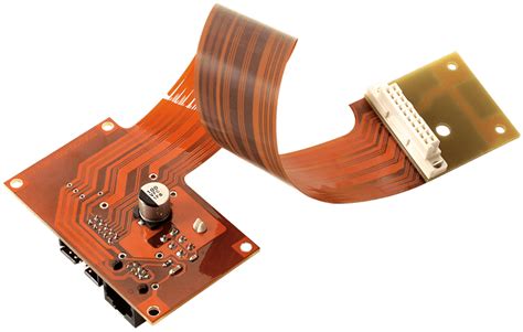
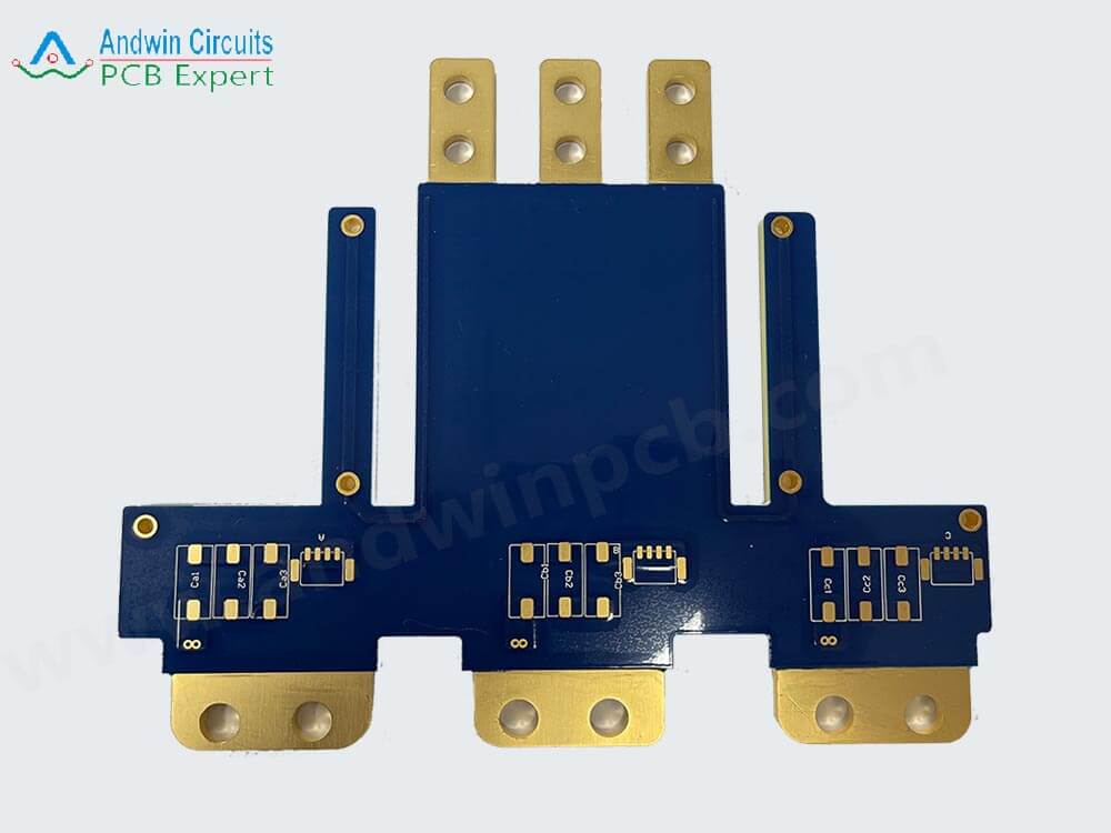
Embedded copper coin pcb
Benefits Of Embedded Copper Coin PCB In High-Power Applications
Embedded copper coin PCBs have emerged as a pivotal innovation in the realm of high-power applications, offering a multitude of benefits that address the growing demands for efficiency, reliability, and thermal management. As electronic devices continue to evolve, the need for robust solutions that can handle increased power densities without compromising performance has become paramount. Embedded copper coin PCBs, with their unique construction and material properties, provide an effective answer to these challenges.
One of the primary advantages of embedded copper coin PCBs is their exceptional thermal conductivity.
In high-power applications, managing heat dissipation is crucial to maintaining the integrity and longevity of electronic components. Traditional PCBs often struggle with heat management, leading to potential overheating and subsequent failure of the device. However, the integration of copper coins within the PCB structure significantly enhances thermal performance. Copper, known for its excellent thermal conductivity, efficiently transfers heat away from critical components, thereby reducing the risk of thermal-related issues and ensuring stable operation even under demanding conditions.
Moreover, embedded copper coin PCBs contribute to improved electrical performance.
High-power applications often require the handling of substantial current loads, which can lead to increased resistance and potential signal loss in conventional PCBs. The incorporation of copper coins mitigates these issues by providing a low-resistance path for current flow. This not only enhances the overall electrical efficiency but also minimizes power losses, resulting in more reliable and energy-efficient systems. Consequently, devices utilizing embedded copper coin PCBs can achieve higher performance levels while maintaining optimal power consumption.
In addition to thermal and electrical benefits, embedded copper coin PCBs offer superior mechanical stability.
High-power applications frequently involve harsh operating environments, where mechanical stress and vibrations are common. The robust construction of copper coins embedded within the PCB adds structural integrity, making the entire assembly more resilient to physical stresses. This increased durability translates to a longer lifespan for the device, reducing the need for frequent maintenance or replacements and thereby lowering the total cost of ownership.
Furthermore, the design flexibility afforded by embedded copper coin PCBs cannot be overlooked.
Engineers and designers can strategically place copper coins in areas where heat generation is most significant, allowing for targeted thermal management. This level of customization ensures that each application can be optimized for its specific requirements, enhancing overall system performance. Additionally, the compact nature of embedded copper coins allows for more efficient use of space within the PCB, enabling the development of smaller, more compact devices without sacrificing functionality or reliability.
Transitioning to the manufacturing perspective, embedded copper coin PCBs are compatible with standard PCB fabrication processes, which facilitates their integration into existing production lines.
This compatibility not only streamlines the manufacturing process but also reduces production costs, making this advanced technology accessible to a broader range of applications. As a result, industries such as automotive, telecommunications, and consumer electronics can leverage the benefits of embedded copper coin PCBs to enhance their products’ performance and reliability.
In conclusion, the adoption of embedded copper coin PCBs in high-power applications offers a multitude of benefits that address critical challenges in thermal management, electrical performance, mechanical stability, and design flexibility. By efficiently dissipating heat, reducing electrical resistance, and providing robust structural support, these advanced PCBs enable the development of more reliable, efficient, and compact electronic devices. As technology continues to advance, the role of embedded copper coin PCBs in high-power applications is poised to become increasingly significant, driving innovation and performance across various industries.
Manufacturing Process Of Embedded Copper Coin PCB
The manufacturing process of embedded copper coin PCBs is a sophisticated and intricate procedure that demands precision and expertise. This advanced technology is increasingly being adopted in various high-performance electronic applications due to its superior thermal management capabilities. To understand the manufacturing process, it is essential to delve into the sequential steps that ensure the production of high-quality embedded copper coin PCBs.
Initially, the process begins with the selection of appropriate materials.
High-quality copper and substrate materials are chosen to ensure optimal performance and durability. The copper coins, which are essentially small, thick pieces of copper, are meticulously prepared to be embedded into the PCB. These copper coins play a crucial role in dissipating heat generated by high-power components, thereby enhancing the overall reliability and efficiency of the electronic device.
Following the material selection, the next step involves the design and layout of the PCB.
Advanced computer-aided design (CAD) software is employed to create precise and detailed layouts. This design phase is critical as it determines the placement of the copper coins and the overall configuration of the PCB. Engineers must ensure that the design meets the specific thermal and electrical requirements of the application.
Once the design is finalized, the manufacturing process moves to the drilling stage.
Precision drilling machines are used to create holes in the PCB substrate where the copper coins will be embedded. These holes must be accurately positioned and sized to accommodate the copper coins snugly. Any deviation in this step can lead to poor thermal performance and potential failure of the PCB.
After drilling, the copper coins are carefully inserted into the pre-drilled holes.
This embedding process requires meticulous attention to detail to ensure that the copper coins are properly aligned and securely placed. The coins must make good contact with the surrounding substrate to facilitate efficient heat transfer. To achieve this, a combination of mechanical and thermal techniques is often employed.
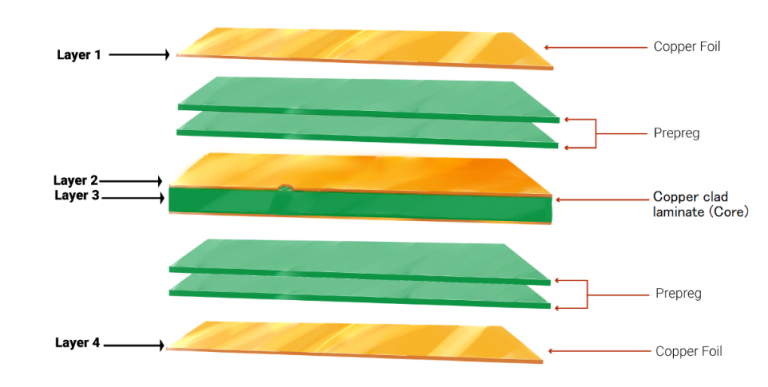
Subsequently, the PCB undergoes a lamination process.
During lamination, layers of insulating material and copper foil are pressed together under high temperature and pressure. This step not only secures the embedded copper coins in place but also forms the multilayer structure of the PCB. The lamination process is crucial for ensuring the structural integrity and electrical performance of the final product.
Following lamination, the PCB is subjected to a series of etching and plating processes.
These processes involve the removal of excess copper and the deposition of additional copper layers to form the desired circuit patterns. The embedded copper coins are integrated into these patterns, providing localized thermal management where it is most needed. The precision of these processes is paramount to achieving the desired electrical characteristics and performance.
Finally, the PCB undergoes rigorous testing and inspection to ensure its quality and functionality.
Advanced testing equipment is used to verify the electrical performance, thermal management capabilities, and overall reliability of the PCB. Any defects or inconsistencies are identified and rectified before the PCB is approved for use.
In conclusion, the manufacturing process of embedded copper coin PCBs is a complex and meticulous procedure that involves multiple stages, from material selection and design to drilling, embedding, lamination, etching, and testing. Each step is critical to ensuring the production of high-quality PCBs that meet the demanding requirements of modern electronic applications. Through this intricate process, embedded copper coin PCBs provide superior thermal management and enhanced performance, making them an invaluable component in the electronics industry.
Thermal Management Solutions Using Embedded Copper Coin PCB
In the ever-evolving landscape of electronics, thermal management has emerged as a critical concern for engineers and designers. As devices become more compact and powerful, the need for efficient heat dissipation solutions has never been more pressing. One innovative approach that has gained traction in recent years is the use of embedded copper coin PCBs. This technology offers a promising solution to the thermal challenges faced by modern electronic devices.
Embedded copper coin PCBs are designed to enhance thermal conductivity within a printed circuit board (PCB).
By integrating a copper coin directly into the PCB, this method provides a direct thermal path from the heat-generating components to the heat sink. This direct path significantly reduces thermal resistance, thereby improving the overall thermal performance of the device. The copper coin acts as a heat spreader, distributing heat more evenly and efficiently across the PCB.
The advantages of using embedded copper coin PCBs are manifold.
Firstly, they offer superior thermal conductivity compared to traditional thermal management solutions. Copper, known for its excellent thermal properties, ensures that heat is rapidly conducted away from critical components. This is particularly beneficial in high-power applications where excessive heat can lead to performance degradation or even failure. By maintaining optimal operating temperatures, embedded copper coin PCBs help extend the lifespan of electronic devices.
Moreover, embedded copper coin PCBs contribute to the miniaturization of electronic devices.
As the demand for smaller, more powerful gadgets continues to rise, the need for compact thermal management solutions becomes paramount. Traditional methods, such as heat sinks and thermal pads, often occupy valuable space within the device. In contrast, embedded copper coins are integrated directly into the PCB, eliminating the need for additional components and allowing for more streamlined designs. This integration not only saves space but also reduces the overall weight of the device, making it more portable and user-friendly.
In addition to their thermal benefits, embedded copper coin PCBs also offer mechanical advantages.
The copper coin provides structural support to the PCB, enhancing its durability and reliability. This is particularly important in applications where the device is subjected to mechanical stress or vibration. The added rigidity helps prevent damage to the PCB and ensures consistent performance over time.
Despite these advantages, the implementation of embedded copper coin PCBs does come with certain challenges.
The manufacturing process is more complex and requires precise control to ensure proper integration of the copper coin. This can lead to higher production costs compared to traditional PCBs. However, the long-term benefits in terms of improved thermal performance and device reliability often outweigh the initial investment.
Furthermore, the design of embedded copper coin PCBs requires careful consideration of various factors, such as the placement of the copper coin and the thermal properties of the surrounding materials. Engineers must conduct thorough thermal analysis to optimize the design and ensure effective heat dissipation. Collaboration between designers, manufacturers, and thermal experts is essential to achieve the desired performance outcomes.
In conclusion, embedded copper coin PCBs represent a significant advancement in thermal management solutions for modern electronic devices. By leveraging the superior thermal conductivity of copper and integrating it directly into the PCB, this technology addresses the critical issue of heat dissipation in a compact and efficient manner. While the implementation may pose certain challenges, the benefits in terms of enhanced thermal performance, device miniaturization, and mechanical durability make embedded copper coin PCBs a compelling choice for the future of electronics. As the industry continues to push the boundaries of innovation, it is likely that we will see even more sophisticated applications of this technology in the years to come.
Design Considerations For Embedded Copper Coin PCB
When designing an embedded copper coin PCB, several critical considerations must be taken into account to ensure optimal performance and reliability. The integration of copper coins into PCBs is primarily driven by the need for enhanced thermal management, particularly in high-power applications where heat dissipation is crucial. Therefore, understanding the thermal requirements of the application is the first step in the design process. By accurately assessing the thermal load, designers can determine the appropriate size, shape, and placement of the copper coins to effectively manage heat.
Transitioning from thermal considerations, the mechanical aspects of the PCB design also play a significant role.
The inclusion of copper coins can impact the structural integrity of the PCB, necessitating careful planning to avoid potential issues such as warping or delamination. It is essential to ensure that the copper coins are securely embedded within the PCB substrate, maintaining a robust connection that can withstand mechanical stresses during both the manufacturing process and the operational life of the device.
In addition to thermal and mechanical factors, electrical performance must be meticulously evaluated.
Copper coins can influence the electrical characteristics of the PCB, including impedance and signal integrity. Designers must account for these changes by adjusting the layout and routing of traces to minimize any adverse effects. This often involves detailed simulations and modeling to predict the behavior of the PCB under various operating conditions, ensuring that the final design meets the required electrical specifications.
Furthermore, the choice of materials is another critical consideration in the design of embedded copper coin PCBs.
The compatibility of the copper coins with the PCB substrate material is paramount to prevent issues such as galvanic corrosion or poor adhesion. Selecting materials with similar thermal expansion coefficients can mitigate the risk of mechanical failure due to thermal cycling. Additionally, the thermal conductivity of the substrate material should complement the heat dissipation capabilities of the copper coins, creating a synergistic effect that enhances overall thermal management.
Manufacturing processes also need to be carefully planned and executed to achieve a high-quality embedded copper coin PCB.
The precision required in embedding copper coins necessitates advanced fabrication techniques and stringent quality control measures. Any misalignment or improper embedding can compromise the performance and reliability of the PCB. Therefore, collaboration with experienced manufacturers who possess the necessary expertise and equipment is crucial to the success of the project.
Moreover, cost considerations cannot be overlooked in the design process.
While embedded copper coin PCBs offer significant performance benefits, they can also increase the overall cost of the PCB due to the additional materials and manufacturing complexity involved. Designers must balance the performance gains with the budget constraints of the project, exploring cost-effective solutions without compromising on quality and reliability.
Finally, environmental and regulatory compliance is an essential aspect of the design process.
Ensuring that the materials and manufacturing processes used in the production of embedded copper coin PCBs adhere to relevant environmental standards and regulations is vital. This not only helps in meeting legal requirements but also promotes sustainability and reduces the environmental impact of the product.
In conclusion, the design of embedded copper coin PCBs involves a multifaceted approach that encompasses thermal management, mechanical integrity, electrical performance, material selection, manufacturing precision, cost considerations, and regulatory compliance. By carefully addressing each of these factors, designers can create high-performance PCBs that meet the demanding requirements of modern electronic applications.