EMC circuit design related
1.Key points of EMC circuit filter design:
L1 is a common-mode inductor, which can attenuate common-mode interference, suppress interference inside the board and external interference, improve the product’s anti-interference ability, and reduce external radiation through the 429 signal line. The common-mode inductor impedance selection range is 120Ω/100MHz ~2200Ω/100MHz, and the typical value is 1000Ω/100MHz;
C1 and C2 are filter capacitors, which provide a low-impedance return path for interference, effectively reduce external common-mode current and filter external interference at the same time; the capacitance value selection range is 22PF~1000pF, and the typical value is 100pF; if the signal line has insulation withstand voltage requirements for the metal shell, then the two filter capacitors of the differential line to the ground need to consider withstand voltage;
When there are multiple nodes on the circuit, consider reducing or removing the value of the filter capacitor. C3 is the jumper capacitor between the interface ground and the digital ground, with a typical value of 1000pF, The capacitance of C3 can be adjusted according to the test situation;
2.Key points of EMC circuit lightning protection design:
In order to meet the lightning protection test requirements of IEC61000-4-5 or GB17626.5 standards, common mode 6KV, differential mode 2KV, D4 is a three-terminal gas discharge tube to form the first-level protection circuit, which is used to suppress the common mode and differential mode surge interference on the line to prevent interference from affecting the next level circuit through the signal line;
The nominal voltage VBRW of the gas discharge tube is required to be greater than 13V, and the peak current IPP is required to be greater than or equal to 143A;
The peak power WPP is required to be greater than or equal to 1859W;
PTC1 and PTC2 are thermistors to form the second-level protection circuit, with a typical value of 10Ω/2W;
To ensure the gas discharge The electric tube can be smoothly turned on. To discharge a large amount of energy, this resistor must be added for voltage division to ensure that most of the energy goes away through the gas discharge tube;
D1~D3 are TSS tubes (semiconductor discharge tubes) to form the third-level protection circuit. The nominal voltage VBRW of the TSS tube is required to be greater than 8V, the peak current IPP is required to be greater than or equal to 143A; the peak power WPP is required to be greater than or equal to 1144W;
Interface circuit design notes:
If the device is a metal shell, and the single board can independently divide the interface ground, then the metal shell is directly electrically connected to the interface ground, and the single board ground is connected to the interface ground through a 1000pF capacitor;
If the device is a non-metallic shell, then the interface ground PGND is directly electrically connected to the single board digital ground GND.
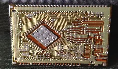
3.IC sockets should not be used for EMC
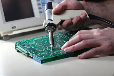
IC sockets are very unfavorable to EMC. It is recommended to directly solder surface-mount chips on PCBs. IC chips with shorter leads and smaller volumes are better. BGA and similar chip packaging ICs are currently the best choice. The emission and sensitivity of a PROM mounted on a socket (or worse, a socket with a battery) often ruins an otherwise good design. Therefore, a surface mount PROM soldered directly to the board should be used.
Motherboards with ZIF sockets and spring-mounted heat sinks on the processor (which can be easily upgraded) require additional filtering and shielding, but even so, it is beneficial to choose a surface mount ZIF socket with the shortest internal leads.
4.EMC circuit design
- Use level detection (not edge detection) for inputs and buttons
- Use digital signals with the slowest and smoothest leading edge rate (without exceeding the distortion limit)
- On PCB samples, allow control of signal edge speed or bandwidth (for example, use soft ferrite beads or series resistors on the driver end)
- Reduce load capacitance to make the open collector driver close to the output easy to pull up, and the resistance value is as large as possible * The processor heat sink is isolated from the chip by thermal conductive material, and multiple RF grounding is performed around the processor.
- High-quality RF bypassing (decoupling) of the power supply is important at each power pin.
- High-quality power monitoring circuits need to be resistant to power interruptions, drops, surges and transient interference
- A high-quality watchdog is required
- Never use programmable devices on watchdog or power monitoring circuits
- Power monitoring circuits and watchdogs also need appropriate circuit and software techniques to make them adaptable to most unexpected situations, depending on the critical state of the product
- When the rise/fall time of the logic signal edge is shorter than the time it takes for the signal to transmit a round trip in the PCB trace, transmission line technology should be used:
a. Experience: The time it takes for the signal to transmit a round trip in each millimeter of track length is equal to 36 picoseconds
b. For the best EMC characteristics, use transmission line technology for tracks that are much shorter than the experience in a Some digital ICs generate high-level radiation, and their matching small metal boxes are often soldered to the PCB ground to achieve shielding effect. Shielding on PCBs is low cost, but it is not applicable to devices that require heat dissipation and good ventilation.
The clock circuit is usually the main source of emission, and its PCB track is the most critical point. The layout of the components should be done well to make the clock routing as short as possible, while ensuring that the clock line is on one side of the PCB but not through the vias. When a clock must go through a long path to reach many loads, a clock buffer can be installed next to the load, so that the current in the long track (wire) is much smaller. Here, relative distortion is not important. The clock edge in the long track should be as smooth as possible, and even a sine wave can be used, and then shaped by the clock buffer next to the load.