EMS PCB Strategies for Modern Electronics Manufacturing
Key Takeaways
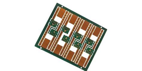
Modern EMS PCB strategies are reshaping electronics manufacturing by combining smart design principles with cutting-edge IoT integration. These approaches enable manufacturers to address evolving demands for scalability, reliability, and cost efficiency. At the core of this transformation lies PCB assembly (PCBA) optimization, where advanced techniques like automated component placement and AI-driven defect detection are minimizing errors by up to 40% compared to traditional methods.
A critical advancement is the shift toward modular design frameworks, which allow PCB assembly lines to adapt swiftly to product iterations. For instance, embedding IoT sensors directly into PCBA workflows provides real-time analytics on thermal performance and solder joint integrity, reducing post-production failures by 25–30%.
| Traditional Approach | Modern EMS Strategy | Performance Gain |
|---|---|---|
| Manual design validation | AI-powered simulation tools | 50% faster iteration |
| Fixed production layouts | Modular PCBA systems | 35% higher scalability |
| Reactive quality checks | Predictive IoT monitoring | 22% fewer defects |
To enhance cost-effectiveness, manufacturers are adopting dual-track strategies: optimizing PCB assembly material usage through generative design algorithms while standardizing testing protocols across PCBA stages. This hybrid model cuts prototyping costs by 18–20% without compromising reliability.
Furthermore, edge computing integration in EMS PCB processes enables localized data processing, reducing latency in defect detection during high-speed PCB assembly. Paired with blockchain-enabled traceability systems, this ensures compliance with stringent industry standards while future-proofing supply chain transparency.
By prioritizing interoperability between design software and PCBA machinery, forward-thinking EMS providers are achieving 95% first-pass yield rates—a 15% improvement over legacy systems. These innovations underscore the importance of aligning PCB assembly workflows with Industry 4.0 principles to maintain competitiveness in dynamic markets.
Smart Design Innovations in EMS PCB
Modern PCB assembly processes are undergoing transformative shifts as EMS providers integrate smart design principles to address evolving electronics demands. By leveraging PCBA-optimized workflows, manufacturers now prioritize design-for-manufacturability (DFM) frameworks that reduce prototyping cycles by up to 40%. For instance, AI-driven layout tools analyze component placement for thermal efficiency, minimizing signal interference risks while accelerating time-to-market.
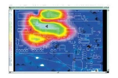
Tip: Implementing simulation-driven design early in the PCBA phase can preemptively identify thermal hotspots, reducing post-production rework costs by 15–22%.
A key advancement lies in modular design architectures, enabling rapid customization for IoT and edge-computing applications. These frameworks allow EMS partners to reuse validated circuit blocks across product lines, cutting development timelines by 30%. Additionally, embedded testing protocols are now integrated directly into PCB assembly workflows, automating defect detection during solder paste application and component mounting.
The adoption of additive manufacturing for PCBA substrates further exemplifies innovation. 3D-printed circuits with embedded sensors enable real-time performance monitoring, enhancing reliability in harsh environments. Combined with IoT-enabled traceability systems, manufacturers achieve end-to-end visibility, ensuring compliance with aerospace and medical-grade standards.
“Collaboration between design and manufacturing teams is critical. Over 68% of efficiency gains in EMS PCB projects stem from cross-functional DFM reviews,” notes a recent industry whitepaper.
To balance scalability with precision, EMS providers are deploying hybrid models that pair automated PCB assembly lines with AI-driven quality analytics. This approach reduces human error in microcomponent placement while supporting high-mix, low-volume production—a necessity for agile electronics ecosystems. By unifying smart design with data-driven processes, the industry is redefining how PCBA innovations meet tomorrow’s technological challenges.
IoT Integration for PCB Manufacturing Efficiency
The integration of IoT (Internet of Things) into PCB assembly processes is redefining efficiency benchmarks in modern electronics manufacturing. By embedding smart sensors and connected devices across PCBA production lines, manufacturers gain real-time visibility into critical parameters such as temperature, humidity, and component placement accuracy. This data-driven approach enables predictive maintenance, reducing downtime by identifying equipment anomalies before they escalate. For instance, IoT-enabled systems can autonomously adjust reflow oven temperatures based on live thermal feedback, ensuring optimal solder joint quality while minimizing material waste.
Beyond operational monitoring, IoT facilitates seamless communication between PCB assembly stages. Automated guided vehicles (AGVs) equipped with IoT sensors streamline material flow from inventory to pick-and-place machines, synchronizing workflows without manual intervention. This closed-loop coordination is particularly vital for high-mix, low-volume production, where rapid changeovers demand precise timing. Additionally, cloud-based analytics platforms aggregate data from distributed PCBA facilities, empowering manufacturers to benchmark performance metrics and replicate best practices globally.
Scalability is another cornerstone of IoT-driven PCB manufacturing. As order volumes fluctuate, modular IoT architectures allow factories to dynamically scale sensor networks and data-processing capabilities. For example, adding edge computing nodes to existing PCBA lines can enhance local data analysis speeds, enabling faster decision-making without overloading central servers. This adaptability not only future-proofs infrastructure but also supports compliance with evolving industry standards, such as traceability requirements for automotive or medical electronics.
By merging IoT with advanced EMS PCB strategies, manufacturers achieve a dual advantage: elevated productivity and uncompromised reliability. Real-time defect detection algorithms, powered by machine learning models fed with IoT data, can flag deviations in component alignment or solder paste deposition within milliseconds. This shift from reactive to proactive quality control slashes rework rates by up to 40%, directly boosting profitability. As the electronics industry pivots toward smarter, interconnected ecosystems, IoT integration remains a non-negotiable lever for sustaining competitive PCB assembly workflows.

Scalable EMS Solutions for Electronics Growth
The demand for adaptable manufacturing systems has never been higher as electronics markets evolve at breakneck speeds. PCB assembly processes now require architectures that can seamlessly scale to accommodate fluctuating production volumes, design iterations, and emerging technologies. Modern scalable EMS frameworks leverage modular PCBA workflows, enabling manufacturers to pivot between high-mix, low-volume prototyping and mass production without compromising turnaround times. By integrating IoT-driven monitoring into PCB assembly lines, EMS providers gain real-time visibility into capacity utilization, allowing dynamic adjustments to meet spikes in demand or shifts in component availability.
A critical enabler of scalability lies in the adoption of hybrid manufacturing models. For instance, combining automated PCBA lines with flexible, reconfigurable tooling ensures rapid adaptation to design changes—a necessity in industries like automotive or wearable tech. Advanced planning systems further enhance this agility, using predictive analytics to optimize material procurement and inventory buffers for high-risk components, such as specialized ICs or connectors. This approach minimizes bottlenecks while maintaining cost efficiency across scaled operations.
Another pillar of scalable EMS solutions is the emphasis on supply chain resilience. By establishing distributed PCB assembly hubs and qualifying multiple component suppliers, manufacturers reduce geographic and logistical dependencies. Cloud-based collaboration platforms further streamline communication between design teams, PCBA partners, and end clients, ensuring alignment even as project scopes expand. For example, a medical device startup scaling from pilot batches to full production can maintain consistency in quality and compliance through standardized EMS protocols applied across all manufacturing nodes.
Finally, scalability extends to post-production phases. Modular testing rigs and upgradable firmware programming stations allow EMS providers to future-proof PCB assembly outputs. This is particularly vital for IoT devices, where over-the-air update capabilities demand forward-compatible hardware designs. By embedding scalability into every layer of the manufacturing process—from component sourcing to final validation—EMS partners empower electronics brands to navigate market uncertainties while capitalizing on growth opportunities.
Optimizing PCB Reliability With EMS Tech
In the high-stakes world of electronics manufacturing, PCB reliability hinges on precision-driven EMS PCB strategies. By leveraging advanced pcb assembly methodologies, EMS providers ensure that every pcba (printed circuit board assembly) meets rigorous performance benchmarks. Automated optical inspection (AOI) systems, for instance, scan boards at micron-level resolutions to detect solder defects or misaligned components, reducing field failure rates by up to 40%. Similarly, design for manufacturability (DFM) principles are integrated early in the development cycle to eliminate layout flaws that could compromise long-term functionality.
Material selection plays a pivotal role in enhancing durability. High-performance substrates like polyimide or ceramic-filled laminates are paired with pcb assembly processes optimized for thermal management, ensuring stability in extreme operating conditions. Advanced thermal cycling tests simulate years of stress within hours, validating resilience against expansion-contraction cycles. EMS partners also employ failure mode and effects analysis (FMEA) to preemptively address risks, from solder joint fatigue to copper trace delamination.
For pcba projects requiring scalability, EMS workflows incorporate traceability protocols that track components from sourcing to final testing. This not only streamlines compliance with industry standards like IPC-A-610 but also accelerates root-cause analysis if anomalies arise. Real-time data analytics further refine processes, with machine learning algorithms predicting wear patterns and recommending design tweaks before production ramps up.
Transitioning to IoT-enabled systems, EMS providers now embed environmental sensors directly into PCB assembly lines. These sensors monitor humidity, temperature, and vibration during manufacturing, ensuring ambient conditions never deviate from optimal parameters. Such granular control is critical for applications in aerospace or medical devices, where a single flaw can have catastrophic consequences.
By unifying smart design, rigorous testing, and data-driven oversight, EMS technology transforms pcba reliability from an aspirational goal into a measurable outcome—future-proofing electronics against evolving operational demands.
EMS Strategies for Cost-Effective PCB Production
Achieving cost efficiency in PCB assembly requires a holistic approach that balances technical precision with strategic resource management. A foundational strategy involves design-for-manufacturability (DFM) principles, which optimize board layouts to minimize material waste and reduce PCBA cycle times. By collaborating early with design engineers, EMS providers can identify opportunities to standardize components, simplify routing patterns, and eliminate redundant test points—directly lowering bill-of-materials (BOM) costs by 12–18% in typical applications.
Automation plays a pivotal role in scaling PCB assembly workflows without compromising quality. Selective soldering robots and AI-driven optical inspection systems enable first-pass yield improvements of up to 40%, significantly reducing rework expenses. For high-mix production environments, modular PCBA lines with quick-change tooling adapters cut equipment downtime by 30%, allowing manufacturers to pivot between product variants without costly recalibration delays.
Material procurement strategies further amplify cost savings. EMS partners leveraging consolidated purchasing power secure better pricing for high-demand ICs and connectors, while vendor-managed inventory systems prevent overstocking of obsolete parts. Advanced lifecycle forecasting tools help manufacturers phase out aging components 6–8 months before discontinuation, avoiding last-minute redesign costs.
Energy efficiency initiatives, such as transitioning to lead-free soldering processes with lower thermal requirements, reduce power consumption in PCB assembly by 22–25%. Combined with waste heat recovery systems, these measures align with circular economy principles while trimming operational budgets.
To maintain cost competitiveness without sacrificing reliability, tier-one EMS providers implement predictive maintenance protocols for PCBA equipment. Vibration sensors and thermal imaging cameras detect potential machine failures 72+ hours in advance, preventing unplanned stoppages that cost manufacturers an average of $5,400 per hour in lost productivity.
These strategies collectively create a value cascade—where design optimizations enable manufacturing efficiencies, which in turn drive supply chain improvements—delivering sustained cost reductions of 15–30% across the PCB assembly lifecycle.
Advanced PCB Manufacturing Techniques in EMS
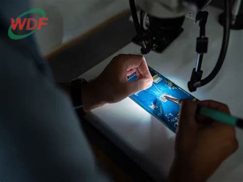
Modern electronics manufacturing demands precision, scalability, and adaptability, driving EMS providers to adopt cutting-edge PCB assembly methods. By leveraging automated robotic systems for high-precision component placement, manufacturers achieve micron-level accuracy in PCBA processes, minimizing human error and enhancing throughput. Advanced techniques like laser direct imaging (LDI) enable finer trace widths, critical for high-density interconnect (HDI) boards used in IoT devices and wearables.
The integration of additive manufacturing allows for rapid prototyping of complex PCB geometries, reducing time-to-market for next-gen electronics. For instance, 3D-printed circuit structures are increasingly used in aerospace and medical devices, where compact, lightweight designs are paramount. Additionally, automated optical inspection (AOI) and X-ray inspection systems ensure defect detection rates exceeding 99.9%, aligning with stringent quality standards in automotive and industrial applications.
To address thermal management challenges in high-power applications, EMS providers now embed active cooling solutions directly into PCBA layouts. Techniques like embedded copper substrates and thermal vias dissipate heat efficiently, prolonging component lifespan. Furthermore, adaptive soldering technologies—such as vacuum reflow ovens—eliminate voids in ball grid array (BGA) joints, improving reliability in harsh environments.
The shift toward modular production lines enables seamless scaling from low-volume prototypes to mass production. By combining flexible manufacturing systems (FMS) with real-time data analytics, EMS partners optimize material usage and reduce waste, cutting costs by up to 20% in PCB assembly workflows. These innovations not only future-proof manufacturing processes but also ensure compliance with evolving environmental regulations, such as RoHS and REACH.
Transitioning to these advanced methods requires close collaboration between design and manufacturing teams. Model-based engineering (MBE) tools bridge this gap, allowing simulations of PCB performance under real-world conditions before physical production begins. This synergy between digital twinning and advanced fabrication techniques positions EMS as a cornerstone of modern electronics innovation.
Streamlining Quality Control in EMS PCB
Modern PCB assembly processes demand precision at every stage, making streamlined quality control a cornerstone of competitive electronics manufacturing. By integrating automated optical inspection (AOI) systems with machine learning algorithms, EMS providers can detect micron-level defects in PCBA components, reducing human error by up to 70%. Real-time monitoring platforms, synchronized with IoT-enabled production lines, enable immediate adjustments during solder paste application or component placement, ensuring adherence to IPC-A-610 standards.
A critical advancement lies in the adoption of statistical process control (SPC) tools, which analyze data from PCB assembly stages to predict potential failures before they escalate. For instance, thermal profiling during reflow soldering is now optimized using AI-driven models, minimizing warpage and improving PCBA reliability. Cross-functional teams leverage digital twin simulations to validate design-for-manufacturability (DFM) rules, identifying conflicts between CAD layouts and assembly workflows early in the production cycle.
To address scalability challenges, leading EMS firms implement modular testing frameworks that adapt to diverse product lines without requiring hardware reconfiguration. These systems combine boundary-scan testing for embedded systems with flying probe inspections for high-density interconnects, achieving first-pass yield rates exceeding 98%. Additionally, blockchain-based traceability solutions are gaining traction, providing immutable records of material sourcing and PCBA testing results—a vital feature for aerospace and medical device manufacturers.
By unifying these strategies, manufacturers achieve a holistic quality ecosystem that balances speed and accuracy. The result is a 40% reduction in post-production rework cycles and a measurable improvement in mean time between failures (MTBF) for end-use applications. This approach not only meets evolving industry benchmarks but also aligns with sustainable manufacturing goals by minimizing material waste across PCB assembly operations.
Future-Proofing Electronics With EMS PCB
The rapid evolution of consumer demands and technological advancements necessitates electronics that adapt to tomorrow’s challenges. EMS PCB providers address this by embedding scalability and interoperability into every stage of PCB assembly, ensuring products remain relevant amid shifting market dynamics. A cornerstone of this approach is modular design frameworks in PCBA, which allow for seamless component upgrades without overhauling entire systems. For instance, IoT-enabled devices benefit from edge computing modules that can be integrated into existing boards, extending functionality while minimizing redesign costs.
Advanced material selection further enhances longevity. By leveraging high-density interconnect (HDI) technologies and flexible substrates, EMS PCB manufacturers create circuits that withstand mechanical stress and thermal fluctuations common in AI-driven or 5G applications. These innovations are paired with predictive analytics tools that monitor PCBA performance in real time, identifying potential failure points before they impact reliability.
Sustainability is another critical pillar. Forward-thinking EMS PCB strategies prioritize eco-friendly materials, such as halogen-free laminates and lead-free solders, aligning with global regulatory standards like RoHS. This not only reduces environmental footprints but also future-proofs products against tightening compliance requirements.
To ensure scalability, EMS providers employ digital twin simulations during PCB assembly, testing designs under diverse operational scenarios. This virtual prototyping accelerates time-to-market while validating compatibility with emerging technologies, from quantum computing interfaces to next-gen wireless protocols.
Ultimately, the integration of smart manufacturing ecosystems—combining AI-driven process optimization, IoT-enabled supply chains, and agile PCBA workflows—creates a foundation for electronics that evolve alongside technological progress. By balancing innovation with durability, EMS strategies transform printed circuit boards into dynamic assets capable of powering the next decade of breakthroughs.
Conclusion
As the electronics manufacturing landscape evolves, the integration of PCB assembly expertise and PCBA innovations remains pivotal for sustaining competitive advantage. Modern strategies emphasize holistic design-thinking—where IoT-driven analytics intersect with precision manufacturing—to create systems that adapt to dynamic market demands. By prioritizing modular architectures in PCB assembly, manufacturers can achieve both scalability and rapid iteration, essential for industries ranging from automotive to consumer electronics.
The shift toward PCBA processes enhanced by AI-powered quality control underscores a commitment to zero-defect manufacturing, minimizing waste while maximizing throughput. This approach not only elevates product reliability but also aligns with sustainability goals, as optimized material usage reduces environmental impact. Furthermore, the adoption of edge-to-cloud connectivity in PCB assembly workflows enables real-time monitoring, ensuring seamless coordination between design, prototyping, and mass production phases.
Looking ahead, the fusion of agile methodologies with advanced PCBA technologies will continue to redefine electronics manufacturing. Enterprises that leverage these strategies position themselves to navigate supply chain complexities, mitigate risks, and capitalize on emerging opportunities in smart infrastructure and Industry 4.0 ecosystems. By embedding resilience into every layer of PCB assembly, the industry moves closer to a future where innovation and operational excellence coexist seamlessly.
Frequently Asked Questions
How does EMS enhance modern PCB manufacturing processes?
EMS providers leverage advanced PCB assembly techniques combined with real-time monitoring to optimize production workflows. By integrating PCBA design validation tools and automated testing protocols, they reduce errors and accelerate time-to-market for complex electronics.
What role does IoT play in EMS-driven PCB manufacturing?
IoT-enabled sensors embedded during PCB assembly enable predictive maintenance and data-driven process adjustments. This integration allows EMS partners to monitor thermal performance and signal integrity across PCBA units, ensuring consistent quality in high-volume production.
Can EMS solutions scale for startups and large enterprises alike?
Yes, modular PCB assembly frameworks allow EMS providers to adjust production capacity dynamically. Through design-for-manufacturability (DFM) principles and flexible PCBA workflows, manufacturers support both low-volume prototyping and mass production without compromising reliability.
How are cost efficiencies achieved in EMS PCB strategies?
By standardizing component sourcing and adopting unified testing protocols, EMS providers minimize material waste. Advanced PCBA panelization techniques further reduce per-unit costs while maintaining compliance with industry-specific certifications like ISO 9001.
What quality control measures are critical in EMS PCB production?
Automated optical inspection (AOI) and X-ray verification are applied at multiple PCB assembly stages. EMS teams also employ failure mode analysis to preemptively address defects, ensuring PCBA outputs meet stringent reliability benchmarks.
How does EMS future-proof electronics manufacturing?
Proactive adoption of Industry 4.0 standards, such as digital twin simulations for PCBA layouts, allows EMS partners to adapt to emerging technologies. This approach ensures compatibility with next-gen applications like 5G and AI-driven devices.
Explore Customized PCB Assembly Solutions
For tailored PCB assembly services that align with your project’s technical and budgetary needs, please click here. Our PCBA experts are ready to streamline your electronics manufacturing journey.


