Energy Storage System PCB: Design, Challenges, and Future Trends
1. Introduction
Energy storage systems (ESS) play a crucial role in modern power management, renewable energy integration, and electric vehicle (EV) applications. At the heart of these systems lies the Printed Circuit Board (PCB), which ensures efficient power conversion, battery management, and system control. The design and functionality of PCBs in energy storage systems are critical for performance, safety, and reliability.
This article explores the key aspects of energy storage system PCBs, including design considerations, challenges, materials, and future trends.
2. Role of PCBs in Energy Storage Systems
PCBs in energy storage systems serve multiple functions:
- Battery Management System (BMS) PCBs: Monitor cell voltage, temperature, and state of charge (SOC) to ensure safe operation.
- Power Conversion PCBs: Facilitate AC/DC and DC/DC conversion for grid-tied and off-grid systems.
- Control and Communication PCBs: Enable system monitoring, data logging, and remote control via IoT and wireless protocols.
- Protection Circuitry: Prevent overcharging, over-discharging, and short circuits.
Given these roles, PCB design must balance electrical performance, thermal management, and mechanical robustness.
3. Key Design Considerations for ESS PCBs
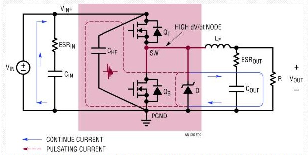
3.1 High Current Handling
Energy storage systems often deal with high currents (up to hundreds of amps). PCB traces must be wide enough to minimize resistive losses and prevent overheating. Techniques include:
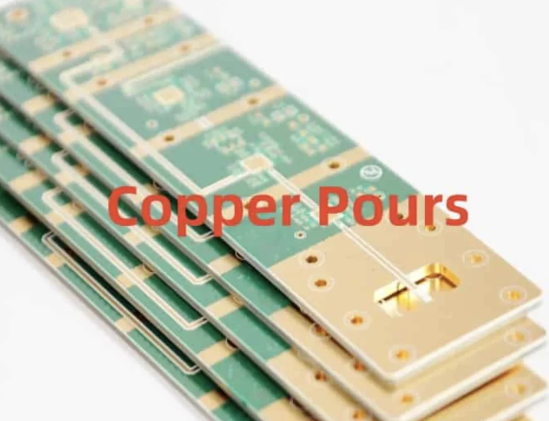
- Thick Copper Layers (2 oz to 6 oz) to reduce resistance.
- Busbars and Heavy Copper PCBs for ultra-high current applications.
- Multi-Layer Stackups to distribute current evenly.
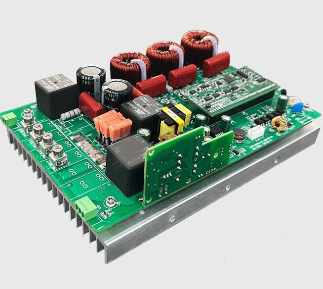
3.2 Thermal Management
Excessive heat degrades performance and lifespan. Effective thermal management strategies include:
- Thermal Vias to dissipate heat from power components.
- Metal-Core PCBs (MCPCBs) for better heat dissipation.
- Heat Sinks and Active Cooling for high-power modules.
3.3 Signal Integrity and Noise Reduction
High-power switching introduces electromagnetic interference (EMI). Mitigation techniques:
- Proper Grounding Schemes (star grounding, ground planes).
- Shielding and Filtering to reduce noise.
- Differential Signaling for communication lines (CAN, SPI, I2C).
3.4 Component Selection
- High-Voltage Components (MOSFETs, IGBTs, capacitors) rated for ESS voltages (48V, 400V, or higher).
- Robust Connectors capable of handling high currents without arcing.
- Isolation Components (optocouplers, transformers) for safety compliance.
3.5 Safety and Compliance
ESS PCBs must meet industry standards such as:
- UL 1973 (Battery Safety Standard)
- IEC 62619 (Industrial Battery Safety)
- IPC-6012 (PCB Reliability Standards)

4. Challenges in ESS PCB Design
4.1 High Voltage Isolation
High-voltage battery stacks require reinforced isolation barriers to prevent leakage currents and arcing. Solutions include:
- Creepage and Clearance Enhancements (wider spacing, slotting).
- Isolation Materials (FR4 with high CTI, polyimide for flexible PCBs).
4.2 Mechanical Stress and Vibration
ESS in EVs and industrial environments face vibrations. Design considerations:
- Conformal Coating to protect against moisture and dust.
- Flex-Rigid PCBs for shock resistance.
- Secure Mounting of heavy components.
4.3 Battery Balancing and Accuracy
BMS PCBs must precisely measure cell voltages (within ±1mV). Challenges include:
- ADC Selection (high-resolution, low-drift ADCs).
- Kalman Filtering for accurate SOC estimation.
- Active vs. Passive Balancing trade-offs.
4.4 Scalability and Modularity
ESS designs must scale for different capacities. Modular PCB architectures allow:
- Stackable BMS Designs for large battery packs.
- Standardized Communication Protocols (CAN, Modbus).
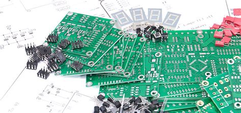
5. Materials and Manufacturing Techniques
5.1 PCB Substrate Materials
- FR4: Standard material for low-cost applications.
- High-Tg FR4: Better thermal resistance for high-power boards.
- Ceramic and Metal-Core PCBs: For extreme thermal conditions.
5.2 Advanced Manufacturing Techniques
- Embedded Components: Reduce parasitic inductance in high-frequency circuits.
- 3D Printing: For prototyping complex geometries.
- Automated Optical Inspection (AOI): Ensures quality in high-volume production.
6. Future Trends in ESS PCBs
6.1 Wide Bandgap Semiconductors (SiC/GaN)
Silicon Carbide (SiC) and Gallium Nitride (GaN) devices enable higher efficiency and power density, reducing PCB thermal stress.
6.2 AI-Optimized BMS
Machine learning algorithms for predictive maintenance and adaptive battery management.
6.3 Wireless BMS
Eliminating wiring harnesses in battery packs using wireless communication (e.g., Tesla’s structural battery pack).
6.4 Sustainable PCB Materials
Bio-based substrates and recyclable materials to reduce environmental impact.
6.5 Integration with Smart Grids
ESS PCBs will incorporate advanced grid-support functions like frequency regulation and demand response.
7. Conclusion
PCBs are the backbone of modern energy storage systems, enabling efficient power management, safety, and scalability. As ESS applications grow—from residential solar storage to grid-scale installations and electric vehicles—PCB designers must address challenges in thermal management, high-current handling, and reliability. Emerging technologies like SiC/GaN semiconductors, AI-driven BMS, and wireless battery management will shape the next generation of ESS PCBs.
By leveraging advanced materials, manufacturing techniques, and smart design practices, engineers can develop PCBs that meet the evolving demands of energy storage systems, contributing to a more sustainable and efficient energy future.