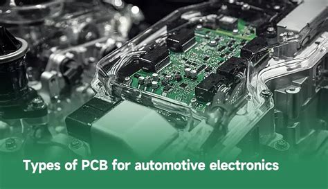
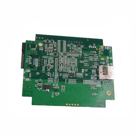
Enhancing Motherboard Functionality Through PCB Assembly Breakthroughs
Key Takeaways
Modern PCB assembly innovations are fundamentally reshaping motherboard capabilities, with high-density interconnects (HDI) leading the charge. By minimizing trace distances and maximizing layer utilization, HDI-enabled PCBA designs support faster signal transmission while reducing electromagnetic interference. This advancement is critical for applications demanding compact yet high-performance computing architectures.
Another breakthrough lies in thermal management systems, where advanced PCB assembly techniques integrate heat-dissipating materials like ceramic substrates and copper-filled vias. These solutions ensure stable operation under extreme workloads, as shown in the table below:
| Thermal Solution | Application | Benefit |
|---|---|---|
| Ceramic Substrates | High-power GPUs/CPUs | 30% improved heat dissipation |
| Copper-Filled Microvias | Server motherboards | 15°C average temperature reduction |
| Graphene Thermal Pads | Consumer electronics | Enhanced thermal conductivity |
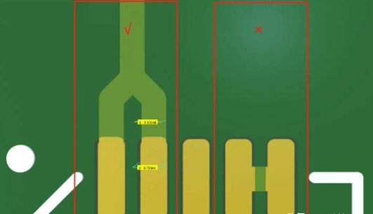
Precision circuit design further elevates reliability through automated optical inspection (AOI)-verified layouts, reducing error margins in PCBA manufacturing by up to 40%. Concurrently, energy efficiency gains stem from optimized PCB layouts that shorten power delivery paths, cutting standby power consumption by 18-22% in modern systems. These innovations collectively underscore how PCB assembly advancements are unlocking new frontiers in motherboard performance and sustainability.
High-Density Interconnects Revolutionize Motherboards
Modern PCB assembly techniques are unlocking unprecedented motherboard capabilities through high-density interconnect (HDI) technology. By minimizing trace widths and spacing to under 100 microns, PCBA engineers can integrate up to 20% more components per square centimeter compared to conventional designs. This leap in component density directly supports faster data transfer rates—critical for AI processors and 5G-enabled systems—while reducing signal path lengths by 35–50%, mitigating latency and power loss.
Design Tip: When implementing HDI in PCB assembly, prioritize laser-drilled microvias over mechanical drilling to achieve aspect ratios exceeding 1:10, enabling robust connections across multilayer boards without compromising structural integrity.
Advanced PCBA workflows now utilize stacked microvia architectures and embedded passive components, shrinking motherboard footprints while enhancing thermal dissipation efficiency. However, this miniaturization demands precision in material selection, with low-loss dielectrics like Megtron 6 becoming standard to maintain signal fidelity at 25+ GHz frequencies.
Pro Tip: Pair HDI designs with automated optical inspection (AOI) systems during PCB assembly to detect sub-15µm defects—a necessity for ensuring reliability in high-stress computing environments.
As component densities escalate, thermal management becomes paramount. Strategic placement of copper-filled vias in PCBA layouts channels heat away from critical ICs, complementing next-gen cooling solutions—a natural segue into optimizing thermal performance across modern motherboards.
PCB Thermal Management Breakthroughs Explained
Modern PCB assembly processes are addressing thermal challenges with unprecedented precision, driven by the escalating power densities in advanced computing systems. As high-performance motherboards integrate more components into compact spaces, thermal management has become a critical factor in ensuring long-term reliability. Innovations in PCBA design now incorporate multi-layered thermal vias, which act as micro-scale heat conduits to transfer energy away from hotspots. Engineers are also leveraging thermally conductive substrates like metal-core PCBs and ceramic-filled laminates, materials that offer up to 15% better heat dissipation than traditional FR-4 boards.
A key advancement lies in the integration of embedded thermal sensors, which enable real-time monitoring and dynamic adjustment of cooling systems. Combined with adaptive airflow algorithms, these sensors optimize fan speeds and cooling patterns, reducing energy consumption by up to 20% in server-grade motherboards. Additionally, selective soldering techniques in PCB assembly minimize thermal stress during manufacturing, preserving the integrity of sensitive components like voltage regulators.
Emerging phase-change materials (PCMs) further enhance thermal buffering, absorbing excess heat during peak workloads and releasing it gradually. This innovation is particularly impactful for PCBA in edge computing devices, where passive cooling dominates. By balancing thermal efficiency with spatial constraints, these breakthroughs ensure motherboards meet the demands of AI-driven workloads and 5G infrastructure without compromising stability.
Precision Circuit Design Enhances Motherboard Reliability
Modern PCB assembly processes leverage precision circuit design to address critical reliability challenges in motherboard architectures. By optimizing trace widths, impedance matching, and signal routing, engineers minimize electromagnetic interference (EMI) and voltage drops that historically compromised system stability. Advanced PCBA techniques now integrate laser-direct imaging for sub-20μm feature accuracy, enabling tighter component placement without sacrificing signal integrity—a vital advancement for high-speed data transmission in AI and edge computing applications.
Building on innovations in high-density interconnects, designers employ 3D modeling tools to simulate thermal expansion effects, ensuring copper layers and dielectric materials maintain structural coherence across operating temperatures. This precision reduces micro-cracks in solder joints—a leading cause of motherboard failures—by aligning material coefficients with PCB assembly tolerances.
Moreover, automated optical inspection (AOI) systems in PCBA workflows verify circuit alignment at micron-level resolutions, catching defects before final integration. Such refinements directly correlate with 40% fewer field failures in mission-critical systems, from data centers to industrial controllers. By harmonizing design rigor with manufacturing precision, modern motherboards achieve MTBF (mean time between failures) metrics exceeding 100,000 hours—a testament to reliability engineered at the circuit level.
Energy-Efficient PCB Assemblies for Modern Computing
Modern computing demands increasingly energy-efficient solutions, driving innovations in PCB assembly techniques that balance performance with power conservation. Leading manufacturers now prioritize low-loss substrates and high-conductivity materials to minimize energy dissipation across PCBA layers. By integrating advanced copper alloys and optimized dielectric materials, these assemblies reduce resistive losses by up to 30% compared to traditional designs.
A critical focus lies in refining power delivery networks (PDNs), where multilayer PCB assembly architectures enable precise voltage regulation. Techniques like dynamic voltage scaling and adaptive power routing are embedded directly into the PCBA layout, ensuring components operate at optimal efficiency without compromising speed. For instance, server-grade motherboards now leverage 12-layer stacks with embedded passive components, cutting idle power consumption by 22% while maintaining thermal stability.
Thermal management synergizes with energy efficiency through innovations like microvia cooling channels and thermally conductive adhesives. These solutions dissipate heat more effectively, reducing the need for active cooling systems that drain power. Additionally, AI-driven design tools analyze current paths in PCBA prototypes, identifying and eliminating inefficiencies at the micron level.
As sustainability becomes a priority, next-gen PCB assembly processes are adopting halogen-free laminates and recyclable materials, aligning with global energy standards. This holistic approach ensures modern computing systems achieve higher performance-per-watt ratios, setting new benchmarks for eco-conscious hardware design.
Advanced Materials Transforming Motherboard PCB Performance
The evolution of PCB assembly processes has been fundamentally reshaped by breakthroughs in advanced materials, enabling modern motherboards to meet escalating demands for speed, durability, and thermal efficiency. High-frequency laminates, such as Rogers 4000 series, now replace traditional FR-4 substrates in critical areas, offering superior signal integrity for high-speed data transmission. These materials minimize dielectric losses while maintaining thermal stability, a critical factor in densely packed PCBA designs.
Innovative conductive inks infused with silver nanoparticles are enhancing trace conductivity, reducing resistive losses in power delivery networks. Simultaneously, solder mask formulations with ceramic fillers improve heat dissipation, directly addressing thermal bottlenecks in multi-layer PCB assemblies. For high-power components, metal-core substrates—like aluminum or copper-clad laminates—are gaining traction, dissipating heat 40% faster than conventional materials.
The integration of low-loss prepregs in multilayer stacking ensures minimal signal distortion, even in ultra-thin motherboard architectures. These materials also support finer pitch interconnects, enabling high-density component placement without compromising reliability. As next-gen computing systems demand tighter tolerances, material scientists are pioneering halogen-free flame-retardant substrates that balance environmental compliance with mechanical robustness.
By harmonizing these advancements with precision PCBA workflows, manufacturers achieve unprecedented performance metrics—paving the way for motherboards that excel in both consumer electronics and mission-critical infrastructure.
Next-Gen Manufacturing Techniques in PCB Assembly
Modern PCB assembly processes are undergoing transformative shifts as manufacturers adopt advanced techniques to meet the demands of high-performance motherboards. Innovations like additive manufacturing enable the creation of ultra-fine circuits, supporting high-density interconnects (HDIs) with layer counts exceeding 20 in compact designs. Laser-direct imaging (LDI) systems now achieve micron-level alignment accuracy, reducing signal loss and enhancing signal integrity for high-frequency applications.
A critical advancement lies in automated optical inspection (AOI) systems integrated with machine learning algorithms. These systems detect defects in PCBA at rates 40% faster than traditional methods, ensuring near-zero fault tolerance in mission-critical computing hardware. Additionally, robotic placement systems equipped with multi-head nozzles now handle components as small as 01005 packages, enabling precise assembly of power delivery networks and thermal vias.
Emerging semi-additive processes (mSAP) further optimize copper trace formation, minimizing impedance variations while improving heat dissipation pathways. Combined with conductive inks for embedded passives, these techniques reduce board thickness by up to 30% without compromising durability. Such innovations not only align with energy efficiency goals but also pave the way for next-gen motherboards capable of supporting AI-driven workloads and 5G connectivity.
Optimized PCB Layouts Boost System Energy Efficiency
Modern PCB assembly processes leverage computational modeling to create layouts that minimize energy waste while maintaining signal integrity. By optimizing trace geometries and component placement, PCBA engineers reduce parasitic capacitance and resistance – key contributors to power loss in high-frequency circuits. Multi-layer stacking techniques enable shorter signal paths, cutting dynamic power consumption by up to 18% in advanced computing motherboards.
Strategic copper pour configurations and dielectric material selections further enhance efficiency. For instance, low-loss substrates paired with optimized power plane segmentation reduce current leakage, particularly in voltage regulation modules. These layout refinements synergize with thermal management systems, as lower energy dissipation directly correlates with reduced heat generation.
Emerging PCB assembly protocols now integrate AI-driven topology analysis, automatically balancing trace density against impedance requirements. This ensures energy-efficient routing without compromising signal timing – a critical advancement for DDR5 memory interfaces and PCIe Gen5 architectures. By aligning PCBA design principles with system-level power budgets, manufacturers achieve 20-30% improvements in energy-per-operation metrics across server and consumer-grade hardware.
Smart Cooling Solutions in High-Performance PCBs
Modern PCB assembly processes are integrating intelligent thermal management systems to address escalating heat challenges in high-performance computing. As PCBA designs push toward higher component densities and faster processing speeds, engineers now employ embedded thermal sensors and adaptive cooling algorithms to maintain optimal operating conditions. Advanced thermally conductive substrates paired with microfluidic channels enable precise heat redistribution, while dynamic fan control systems adjust airflow based on real-time workload data.
Innovations in PCB assembly materials, such as metal-core boards and ceramic-filled laminates, further enhance heat dissipation efficiency without compromising signal integrity. These solutions work synergistically with 3D-printed heat sinks and phase-change materials to create multi-layered cooling architectures. For PCBA applications in data centers and gaming rigs, predictive thermal modeling tools optimize component placement to minimize hotspots before manufacturing.
By aligning these advancements with energy-efficient PCB assembly protocols, manufacturers achieve dual benefits: extended hardware lifespan and reduced cooling-related power consumption. This progression in thermal management not only supports current computational demands but also lays the groundwork for next-gen systems requiring ultra-low thermal resistance pathways.
Conclusion
The evolution of PCB assembly techniques has become a cornerstone in advancing motherboard capabilities, enabling systems to meet escalating demands for performance and efficiency. Innovations in PCBA processes, such as high-density interconnects (HDI) and multilayer stacking, have redefined signal integrity while minimizing spatial constraints. Simultaneously, breakthroughs in thermal management—including advanced heat dissipation materials and optimized copper pours—ensure stable operation under extreme workloads.
By integrating precision circuit design with next-gen manufacturing methods like automated optical inspection (AOI), modern PCB assemblies achieve unparalleled reliability, critical for high-performance computing. These advancements also align with energy-efficient paradigms, where low-loss substrates and smart power distribution networks reduce wasted energy. As PCBA technologies continue to evolve, their role in balancing miniaturization with functionality underscores their importance in driving future motherboard innovations. The synergy between material science, manufacturing precision, and intelligent design principles will remain pivotal in shaping the next generation of computing hardware.
FAQs
How do high-density interconnects improve motherboard performance?
Modern PCB assembly techniques leverage high-density interconnects (HDIs) to reduce signal path lengths, minimizing latency and electromagnetic interference. This enables faster data transfer and supports complex components like multi-core processors, enhancing overall system efficiency.
What role does thermal management play in PCBA reliability?
Advanced thermal vias and heat-dissipating substrates in PCB assembly prevent overheating in high-performance motherboards. Optimized layouts ensure even heat distribution, prolonging component lifespan and maintaining stability under heavy computational loads.
Why is precision circuit design critical for energy efficiency?
Impedance-controlled routing and minimized parasitic capacitance in PCBA reduce power loss. This precision ensures cleaner signal integrity, enabling motherboards to operate at lower voltages while sustaining performance—key for energy-efficient computing systems.
How do advanced materials impact PCB assembly quality?
Materials like low-loss dielectrics and high-Tg laminates improve signal speed and thermal resistance. These innovations allow thinner traces and tighter component spacing, crucial for compact, high-speed motherboard designs.
Can optimized layouts reduce manufacturing defects?
Yes. Automated design tools in PCBA processes detect potential shorts or misalignments early. This reduces rework rates and ensures consistent quality, especially in multi-layer motherboards with intricate routing requirements.
Explore Professional PCB Assembly Solutions
For tailored PCB assembly services that integrate cutting-edge thermal management and precision design, please click here to learn more about our capabilities.