Enig process pcb manufacturing
Introduction To Enig Process PCB Manufacturing
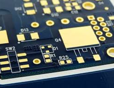
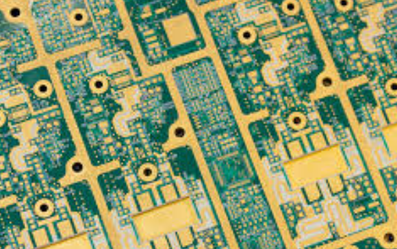
The Electroless Nickel Immersion Gold (ENIG) process is a critical aspect of printed circuit board (PCB) manufacturing, offering a reliable and efficient method for creating high-quality, durable PCBs. This process involves the application of a thin layer of nickel followed by a layer of gold onto the copper pads of a PCB. The ENIG process is highly valued in the electronics industry due to its ability to provide excellent surface planarity, corrosion resistance, and solderability, which are essential for the performance and longevity of electronic devices.
To begin with, the ENIG process starts with the preparation of the PCB surface.
This involves cleaning the copper pads to remove any contaminants, such as oxidation or residues from previous manufacturing steps. A clean surface is crucial for ensuring proper adhesion of the subsequent layers. Following the cleaning process, the PCB is subjected to a micro-etching step, which roughens the copper surface slightly to enhance the bonding of the nickel layer.
Once the surface preparation is complete, the PCB is immersed in an electroless nickel plating bath.
Unlike electroplating, which requires an external electrical current, electroless plating relies on a chemical reduction process to deposit a uniform layer of nickel onto the copper pads. This nickel layer serves as a barrier to prevent the diffusion of copper into the gold layer, which could otherwise lead to poor solderability and reduced reliability of the PCB. The thickness of the nickel layer is typically controlled to be within a range of 3 to 6 micrometers, ensuring adequate protection and performance.
Following the deposition of the nickel layer, the PCB undergoes an immersion gold plating process.
In this step, the PCB is immersed in a gold plating solution, where a thin layer of gold is deposited onto the nickel surface through a chemical displacement reaction. The gold layer, usually around 0.05 to 0.1 micrometers thick, provides excellent corrosion resistance and enhances the solderability of the PCB. The gold also serves as a protective layer, preventing the oxidation of the underlying nickel and ensuring a reliable connection for electronic components.
The ENIG process offers several advantages over other surface finish methods used in PCB manufacturing.
One of the primary benefits is its ability to provide a flat and smooth surface, which is particularly important for fine-pitch components and high-density interconnects. This flatness ensures consistent solder joint formation and reduces the risk of defects such as tombstoning or insufficient solder wetting. Additionally, the ENIG finish is highly resistant to environmental factors, such as humidity and temperature variations, making it suitable for a wide range of applications, from consumer electronics to aerospace and medical devices.
Moreover, the ENIG process is compatible with various assembly techniques, including surface mount technology (SMT) and through-hole technology (THT).
This versatility allows manufacturers to use the same surface finish for different types of components, simplifying the production process and reducing costs. Furthermore, the ENIG finish is lead-free, aligning with global environmental regulations and industry standards, such as the Restriction of Hazardous Substances (RoHS) directive.
In conclusion, the ENIG process is an essential technique in PCB manufacturing, providing a reliable and high-performance surface finish that meets the stringent requirements of modern electronic devices. Its ability to deliver excellent surface planarity, corrosion resistance, and solderability makes it a preferred choice for manufacturers seeking to produce durable and high-quality PCBs. As the demand for advanced electronic devices continues to grow, the ENIG process will remain a cornerstone of PCB manufacturing, ensuring the reliability and performance of the next generation of electronic products.
Benefits Of Using Enig In PCB Fabrication
Electroless Nickel Immersion Gold (ENIG) is a widely adopted surface finish in the realm of Printed Circuit Board (PCB) manufacturing, offering a multitude of benefits that enhance both the performance and reliability of electronic devices. One of the primary advantages of using ENIG in PCB fabrication is its excellent surface planarity. This characteristic is particularly crucial for fine-pitch components and Ball Grid Array (BGA) packages, where even minor surface irregularities can lead to assembly issues and compromised electrical performance. The smooth and flat surface provided by ENIG ensures optimal solderability, thereby facilitating efficient and reliable component placement.
In addition to superior planarity, ENIG offers exceptional corrosion resistance.
The nickel layer acts as a robust barrier, protecting the underlying copper from oxidation and other environmental factors that could degrade the PCB over time. This corrosion resistance is further enhanced by the thin layer of gold, which not only prevents the nickel from tarnishing but also provides a highly conductive surface for soldering. Consequently, PCBs with ENIG finishes exhibit prolonged shelf life and maintain their electrical integrity even in harsh operating conditions.
Another significant benefit of ENIG is its compatibility with various assembly processes.
Unlike some other surface finishes, ENIG is highly versatile and can be used with both leaded and lead-free soldering techniques. This flexibility is particularly advantageous in the current manufacturing landscape, where regulatory requirements and market demands often necessitate the use of lead-free solders. The ability to seamlessly integrate ENIG with different soldering processes simplifies production workflows and reduces the need for multiple surface finish options, thereby streamlining inventory management and reducing costs.
Moreover, ENIG is known for its excellent thermal stability.
The nickel layer can withstand high temperatures without degrading, making it suitable for applications that involve significant thermal cycling or exposure to elevated temperatures. This thermal robustness ensures that the PCB maintains its structural and electrical properties throughout its operational life, thereby enhancing the overall reliability of the electronic device.
Furthermore, the use of ENIG in PCB fabrication contributes to improved signal integrity.
The gold layer provides a low-resistance path for electrical signals, minimizing signal loss and ensuring efficient transmission. This attribute is particularly beneficial for high-frequency applications, where signal integrity is paramount. By reducing signal attenuation and maintaining consistent electrical performance, ENIG-finished PCBs support the development of high-speed and high-performance electronic devices.
In addition to these technical advantages, ENIG also offers environmental benefits.
The electroless plating process used in ENIG is more environmentally friendly compared to some other surface finish techniques, as it typically involves fewer hazardous chemicals and generates less waste. This aligns with the growing emphasis on sustainable manufacturing practices and helps companies meet stringent environmental regulations.
In conclusion, the use of ENIG in PCB fabrication provides a host of benefits that enhance the performance, reliability, and longevity of electronic devices. Its excellent surface planarity, corrosion resistance, compatibility with various assembly processes, thermal stability, and signal integrity make it a preferred choice for many manufacturers. Additionally, its environmental advantages further underscore its suitability in modern PCB manufacturing. As the demand for high-quality and reliable electronic devices continues to grow, the adoption of ENIG as a surface finish is likely to remain a key factor in achieving superior PCB performance.
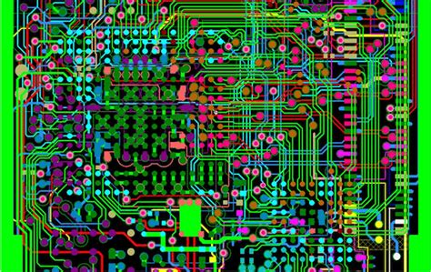
Step-By-Step Guide To Enig PCB Production
The process of Electroless Nickel Immersion Gold (ENIG) PCB manufacturing is a sophisticated and intricate procedure that demands precision and expertise. This method is widely favored in the electronics industry due to its ability to provide a flat, solderable surface and excellent corrosion resistance. To understand the step-by-step guide to ENIG PCB production, it is essential to delve into each stage meticulously, ensuring a comprehensive grasp of the entire process.
Initially, the journey begins with the design phase, where engineers create detailed schematics and layouts using advanced software tools.
These designs are then converted into Gerber files, which serve as the blueprint for the PCB. Following this, the raw material, typically a copper-clad laminate, is prepared. This laminate forms the base of the PCB and is crucial for the subsequent steps.
Subsequently, the laminate undergoes a cleaning process to remove any contaminants that could interfere with the manufacturing process. This is achieved through a series of chemical baths and mechanical scrubbing, ensuring a pristine surface for the next stage. Once cleaned, the laminate is coated with a photosensitive resist material, which is then exposed to ultraviolet light through a photomask. This exposure hardens the resist in the desired pattern, corresponding to the circuit design.
After exposure, the unexposed resist is washed away, revealing the copper beneath.
The next step involves etching, where the exposed copper is removed using a chemical solution, leaving behind the desired copper traces. This etching process is critical, as it defines the electrical pathways on the PCB. Following etching, the remaining resist is stripped away, and the board is cleaned once more to prepare for the drilling phase.
Drilling is performed with high-precision machinery to create holes for component leads and vias, which are essential for electrical connections between different layers of the PCB. These holes are then plated with copper through an electroplating process, ensuring conductivity. The board is subsequently coated with a layer of solder mask, which insulates the copper traces and prevents short circuits. The solder mask is applied using a similar photolithographic process as the resist, ensuring precise application.
The next crucial step is the application of the ENIG finish.
This involves two main stages: electroless nickel plating and immersion gold plating. In the electroless nickel plating stage, the board is submerged in a chemical bath that deposits a uniform layer of nickel onto the exposed copper surfaces. This nickel layer provides a barrier against oxidation and enhances solderability. Following this, the board undergoes immersion gold plating, where a thin layer of gold is deposited onto the nickel surface. The gold layer further protects the nickel from oxidation and provides a highly solderable surface.
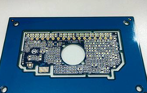
Once the ENIG finish is applied, the board undergoes a series of inspections and tests to ensure quality and functionality.
These tests include electrical testing to verify the integrity of the circuits and visual inspections to check for any defects. If the board passes all tests, it proceeds to the final stage of assembly, where components are mounted and soldered onto the PCB.
In conclusion, the ENIG PCB manufacturing process is a meticulous and multi-faceted procedure that requires careful attention to detail at every stage. From design and preparation to plating and testing, each step is crucial in producing high-quality PCBs that meet the stringent demands of the electronics industry. Through this step-by-step guide, one can appreciate the complexity and precision involved in ENIG PCB production, underscoring its importance in modern electronics manufacturing.
Common Challenges And Solutions In Enig PCB Manufacturing
Electroless Nickel Immersion Gold (ENIG) is a popular surface finish in printed circuit board (PCB) manufacturing due to its excellent solderability, corrosion resistance, and suitability for fine-pitch components. However, the ENIG process is not without its challenges. Understanding these common issues and their solutions is crucial for ensuring high-quality PCB production.
One of the primary challenges in ENIG PCB manufacturing is achieving uniform nickel and gold deposition.
Variations in the thickness of these layers can lead to reliability issues, such as poor solder joint integrity and increased susceptibility to corrosion. To address this, manufacturers must maintain stringent control over the plating bath chemistry and operating conditions. Regular monitoring and adjustment of parameters such as pH, temperature, and chemical concentrations are essential to ensure consistent deposition. Additionally, implementing automated process control systems can help minimize human error and improve overall process stability.
Another significant challenge is the potential for black pad defects, which are characterized by the formation of a dark, brittle layer between the nickel and gold layers. This defect can compromise the mechanical and electrical performance of the PCB. Black pad formation is often attributed to excessive phosphorus content in the nickel layer or improper gold plating conditions. To mitigate this issue, manufacturers should optimize the electroless nickel plating process to achieve the desired phosphorus content and ensure that the immersion gold plating is conducted under controlled conditions. Regular inspection and testing of the plated layers can also help identify and address black pad defects early in the manufacturing process.
Contamination is another common issue in ENIG PCB manufacturing.
Particulate matter, organic residues, and metallic impurities can all adversely affect the quality of the plated layers. To minimize contamination, manufacturers should implement rigorous cleaning protocols for both the PCBs and the plating equipment. This includes thorough rinsing between process steps, using high-purity chemicals, and maintaining a clean working environment. Additionally, periodic maintenance and cleaning of the plating baths and equipment can help prevent the buildup of contaminants.
Adhesion problems between the ENIG finish and the underlying copper substrate can also pose challenges.
Poor adhesion can lead to delamination and reduced reliability of the PCB. To enhance adhesion, it is essential to ensure proper surface preparation of the copper substrate before plating. This typically involves mechanical or chemical cleaning to remove oxides and other contaminants, followed by micro-etching to create a roughened surface that promotes better bonding. Employing adhesion promoters or coupling agents can further improve the adhesion between the copper and the ENIG layers.
Finally, cost considerations are an ongoing challenge in ENIG PCB manufacturing.
The materials and chemicals used in the ENIG process can be expensive, and the need for precise control and monitoring adds to the overall production costs. To address this, manufacturers can explore alternative surface finishes that offer similar performance characteristics at a lower cost. However, it is essential to carefully evaluate the trade-offs in terms of reliability, solderability, and compatibility with fine-pitch components. Additionally, optimizing the ENIG process to reduce waste and improve efficiency can help lower costs without compromising quality.
In conclusion, while ENIG PCB manufacturing presents several challenges, understanding and addressing these issues through careful process control, regular inspection, and rigorous cleaning protocols can significantly enhance the quality and reliability of the final product. By continuously refining their processes and exploring cost-effective alternatives, manufacturers can successfully navigate the complexities of ENIG PCB production and meet the demands of modern electronic applications.