environmental impact of pcb manufacturing
Reducing Toxic Waste in PCB Manufacturing
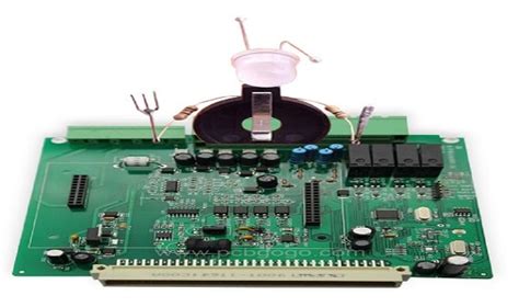
Printed Circuit Board (PCB) manufacturing is a cornerstone of modern electronics, enabling the functionality of devices ranging from smartphones to sophisticated medical equipment.
However, the environmental impact of PCB manufacturing is a growing concern, particularly due to the generation of toxic waste. Addressing this issue requires a multifaceted approach that encompasses technological innovation, regulatory compliance, and industry best practices.
One of the primary sources of toxic waste in PCB manufacturing is the use of hazardous chemicals during the etching and plating processes.
These chemicals, including acids, solvents, and heavy metals, can pose significant risks to both human health and the environment if not managed properly. Consequently, reducing the volume and toxicity of waste generated during these processes is paramount. Advances in chemical recycling and waste treatment technologies offer promising solutions. For instance, closed-loop systems can capture and recycle chemicals, thereby minimizing waste and reducing the need for fresh chemical inputs.
In addition to chemical management, the choice of materials used in PCB manufacturing plays a crucial role in mitigating environmental impact.
Traditional PCBs often contain materials such as lead and brominated flame retardants, which are harmful to the environment. Transitioning to lead-free solder and halogen-free laminates can significantly reduce the toxicity of PCBs. Moreover, the development of biodegradable and recyclable PCB materials is an area of active research, with the potential to further lessen the environmental footprint of electronic devices.
Energy consumption is another critical factor in the environmental impact of PCB manufacturing.
The production process is energy-intensive, contributing to greenhouse gas emissions and climate change. Implementing energy-efficient technologies and practices can help mitigate this impact. For example, optimizing manufacturing processes to reduce energy consumption, investing in renewable energy sources, and improving the energy efficiency of equipment can collectively make a substantial difference. Additionally, adopting Industry 4.0 principles, such as automation and data analytics, can enhance process efficiency and reduce energy waste.
Regulatory frameworks also play a vital role in driving the reduction of toxic waste in PCB manufacturing.
Governments and international bodies have established various regulations and standards aimed at minimizing environmental harm. Compliance with these regulations not only ensures legal adherence but also promotes sustainable practices within the industry. For instance, the Restriction of Hazardous Substances (RoHS) directive in the European Union restricts the use of specific hazardous materials in electronic products, thereby encouraging manufacturers to adopt safer alternatives.
Furthermore, industry collaboration and knowledge sharing are essential for advancing sustainable practices in PCB manufacturing.
Organizations such as the International Electronics Manufacturing Initiative (iNEMI) and the Sustainable Electronics Manufacturing (SEM) working group provide platforms for stakeholders to collaborate on research, share best practices, and develop industry standards. By working together, manufacturers can collectively address common challenges and drive innovation in waste reduction technologies.
Consumer awareness and demand for environmentally friendly products also influence the industry’s approach to toxic waste reduction.
As consumers become more conscious of the environmental impact of their purchases, manufacturers are incentivized to adopt greener practices. Eco-labeling and certification programs can help consumers make informed choices, further driving the market towards sustainability.
In conclusion, reducing toxic waste in PCB manufacturing is a complex but achievable goal that requires concerted efforts across multiple dimensions. By leveraging technological advancements, adhering to regulatory standards, fostering industry collaboration, and responding to consumer demand, the PCB manufacturing industry can significantly mitigate its environmental impact. Through these combined efforts, it is possible to pave the way for a more sustainable future in electronics manufacturing.
Energy Consumption in PCB Production Processes
The environmental impact of printed circuit board (PCB) manufacturing is a multifaceted issue, with energy consumption being a significant contributor. The production processes involved in PCB manufacturing are energy-intensive, encompassing various stages that collectively demand substantial amounts of electricity and other forms of energy. Understanding the energy consumption in these processes is crucial for identifying opportunities to mitigate environmental harm and enhance sustainability.
Initially, the fabrication of PCBs begins with the preparation of raw materials, primarily copper-clad laminates.
The production of these laminates involves the electroplating of copper onto a substrate, a process that requires considerable electrical energy. The energy consumption at this stage is influenced by factors such as the thickness of the copper layer and the efficiency of the electroplating equipment. Consequently, optimizing these parameters can lead to significant energy savings.
Following the preparation of raw materials, the next stage involves the patterning of the PCB, which includes photolithography and etching processes.
Photolithography, a technique used to transfer circuit patterns onto the PCB, relies on ultraviolet (UV) light exposure and chemical development. The energy required for UV light sources and the temperature control of chemical baths contributes to the overall energy footprint. Moreover, the etching process, which removes unwanted copper to create the desired circuit paths, typically employs chemical solutions that must be maintained at specific temperatures, further adding to energy consumption.
Subsequently, the drilling and plating processes are also energy-intensive.
Drilling, which creates holes for electrical connections, utilizes high-speed mechanical drills or laser technology, both of which consume significant amounts of energy. The plating process, essential for creating conductive pathways through these holes, involves electroplating techniques similar to those used in the initial copper-clad laminate preparation. The energy demands of these processes are compounded by the need for precise control and high throughput to meet production standards.
In addition to these primary stages, auxiliary processes such as cleaning, drying, and inspection also contribute to the energy consumption in PCB manufacturing.
Cleaning processes often involve the use of ultrasonic baths or high-pressure sprays, both of which require energy. Drying, typically achieved through convection ovens or infrared heaters, is another energy-intensive step. Inspection processes, which ensure the quality and functionality of the PCBs, may involve automated optical inspection (AOI) systems and X-ray machines, further adding to the energy requirements.
To address the environmental impact of energy consumption in PCB production, manufacturers are increasingly exploring energy-efficient technologies and practices.
For instance, advancements in photolithography equipment that reduce UV light exposure times and improve chemical utilization can lead to lower energy use. Similarly, the adoption of laser drilling technology, which offers higher precision and efficiency compared to mechanical drilling, can result in energy savings. Additionally, implementing energy management systems to monitor and optimize energy use across the production line can help identify areas for improvement and reduce overall consumption.
Furthermore, the integration of renewable energy sources, such as solar or wind power, into the manufacturing process can significantly reduce the carbon footprint associated with energy consumption. By leveraging these sustainable energy sources, PCB manufacturers can not only decrease their environmental impact but also enhance their resilience to energy price fluctuations and regulatory changes.
In conclusion, the energy consumption in PCB production processes is a critical factor contributing to the environmental impact of this industry. By understanding the energy demands at each stage of production and exploring energy-efficient technologies and practices, manufacturers can take meaningful steps towards reducing their environmental footprint and promoting sustainability in PCB manufacturing.
Sustainable Materials for Eco-Friendly PCBs
The environmental impact of printed circuit board (PCB) manufacturing is a growing concern in the electronics industry, prompting a shift towards sustainable materials for eco-friendly PCBs. This transition is not only driven by regulatory pressures but also by the increasing awareness of the environmental footprint associated with traditional PCB production methods. Consequently, the adoption of sustainable materials is becoming a pivotal strategy in mitigating the adverse effects on the environment.
To begin with, conventional PCB manufacturing involves the use of various hazardous chemicals and materials, such as lead, brominated flame retardants, and volatile organic compounds (VOCs). These substances pose significant risks to both human health and the environment. For instance, lead, commonly used in soldering processes, is a toxic metal that can cause severe health issues, including neurological damage. Similarly, brominated flame retardants, while effective in preventing fires, are persistent organic pollutants that can accumulate in the environment and disrupt ecosystems. The release of VOCs during the manufacturing process contributes to air pollution and poses respiratory hazards to workers.
In light of these challenges, the industry is increasingly exploring alternative materials that offer reduced environmental impact.
One promising avenue is the use of lead-free solders, which eliminate the health risks associated with lead exposure. These solders typically contain a combination of tin, silver, and copper, providing comparable performance without the toxic side effects. Additionally, the development of halogen-free flame retardants is gaining traction. These alternatives are designed to meet fire safety standards without the environmental persistence and bioaccumulation issues linked to brominated compounds.
Moreover, the substrate materials used in PCBs are also undergoing a transformation.
Traditional substrates, such as FR-4, are composed of fiberglass and epoxy resins, which are not biodegradable and can release harmful substances during disposal. In contrast, sustainable substrates made from natural fibers, such as cellulose or flax, offer a more eco-friendly option. These materials are not only biodegradable but also renewable, reducing the reliance on finite resources. Furthermore, advancements in bio-based resins, derived from plant sources, are providing viable alternatives to petroleum-based epoxies, further enhancing the sustainability of PCB substrates.
Another critical aspect of sustainable PCB manufacturing is the reduction of waste and the promotion of recycling.
The production process generates significant amounts of waste, including scrap materials and chemical by-products. Implementing closed-loop systems, where waste materials are recovered and reused, can significantly minimize the environmental impact. For example, copper, a primary material in PCBs, can be efficiently recycled, reducing the need for virgin copper extraction, which is both energy-intensive and environmentally damaging.
In addition to material innovations, the industry is also adopting greener manufacturing processes.
Techniques such as additive manufacturing, or 3D printing, offer the potential to reduce material waste and energy consumption. By building PCBs layer by layer, additive manufacturing can achieve precise material usage, minimizing excess and reducing the overall environmental footprint. Furthermore, the use of water-based cleaning agents, as opposed to solvent-based ones, can decrease the release of harmful chemicals into the environment.
In conclusion, the shift towards sustainable materials for eco-friendly PCBs is a multifaceted approach that addresses the environmental impact of traditional manufacturing methods. By adopting lead-free solders, halogen-free flame retardants, biodegradable substrates, and recycling practices, the electronics industry can significantly reduce its ecological footprint. Additionally, the integration of greener manufacturing processes further enhances the sustainability of PCB production. As the industry continues to innovate and prioritize environmental considerations, the transition to eco-friendly PCBs will play a crucial role in fostering a more sustainable future.
Water Usage and Pollution in PCB Manufacturing
The environmental impact of printed circuit board (PCB) manufacturing is a multifaceted issue, with water usage and pollution being significant concerns. The production of PCBs involves several stages, each of which requires substantial amounts of water. This water is used for various purposes, including rinsing, etching, and cleaning the boards. Consequently, the industry’s water consumption is considerable, and the management of this resource is critical to minimizing environmental harm.
To begin with, the etching process in PCB manufacturing is particularly water-intensive.
During this stage, unwanted copper is removed from the board to create the desired circuit patterns. This process necessitates the use of large volumes of water to rinse away the etching chemicals and residues. The water used in this phase often becomes contaminated with heavy metals and other hazardous substances, posing a significant risk to the environment if not properly treated before disposal.
Moreover, the cleaning and rinsing stages also contribute to water pollution.
These steps are essential to ensure that the PCBs are free from any contaminants that could affect their performance. However, the cleaning agents and solvents used can introduce harmful chemicals into the wastewater. If this wastewater is discharged without adequate treatment, it can lead to the contamination of local water bodies, adversely affecting aquatic life and potentially entering the human water supply.
In addition to the direct pollution from chemicals and heavy metals, the high water usage in PCB manufacturing can strain local water resources. In regions where water is already scarce, the industry’s demand can exacerbate shortages, impacting both the environment and local communities. This situation underscores the importance of implementing water conservation measures and efficient water management practices within the industry.
Transitioning to the topic of wastewater treatment, it is crucial to highlight the various methods employed to mitigate the environmental impact of PCB manufacturing. Advanced treatment technologies, such as chemical precipitation, ion exchange, and membrane filtration, are often used to remove contaminants from wastewater. These methods can effectively reduce the concentration of heavy metals and other pollutants, making the water safe for discharge or even reuse in the manufacturing process. However, the implementation of these technologies can be costly, and not all manufacturers may have the resources to invest in such systems.
Furthermore, regulatory frameworks play a vital role in ensuring that PCB manufacturers adhere to environmental standards.
Governments and environmental agencies have established guidelines and limits for the discharge of pollutants, compelling manufacturers to adopt cleaner production techniques and invest in wastewater treatment facilities. Compliance with these regulations is essential to protect water quality and prevent environmental degradation.
In conclusion, the environmental impact of PCB manufacturing, particularly concerning water usage and pollution, is a significant issue that requires concerted efforts from both the industry and regulatory bodies. By adopting advanced treatment technologies, implementing water conservation measures, and adhering to stringent environmental regulations, the industry can mitigate its impact on water resources. This approach not only helps protect the environment but also ensures the sustainability of PCB manufacturing in the long term. As awareness of environmental issues continues to grow, it is imperative for the industry to prioritize sustainable practices and contribute to the global effort to preserve our planet’s precious water resources.