Essential Tips and Tricks for Working with PCB Design Software
Printed Circuit Board (PCB) design is a critical aspect of electronics engineering, requiring precision, efficiency, and attention to detail. Whether you’re a beginner or an experienced designer, mastering PCB design software can significantly enhance your productivity and the quality of your designs. This article explores essential tips and tricks for working with popular PCB design tools such as Altium Designer, KiCad, Eagle, and OrCAD.
1. Mastering Keyboard Shortcuts
Keyboard shortcuts are one of the most effective ways to speed up your workflow. Most PCB design software provides customizable hotkeys that allow you to perform actions quickly without navigating through menus. Here are some commonly used shortcuts across different tools:
- Altium Designer:
- Ctrl + D: Clear all filters
- Shift + S: Toggle single-layer mode
- Q: Toggle between metric and imperial units
- Ctrl + Click & Drag: Move components while maintaining connections
- KiCad:
- M: Move component
- R: Rotate component
- V: Add via
- Ctrl + Z / Ctrl + Y: Undo/Redo
- Eagle:
- Ctrl + F: Find component
- Alt + Click: Measure distance
- Shift + Route: Toggle autorouter
Customizing shortcuts to match your workflow can further improve efficiency.
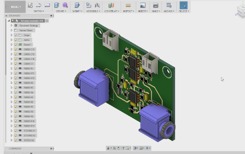
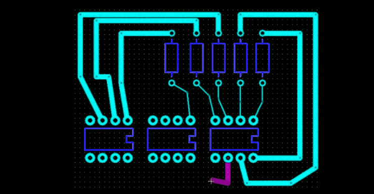
2. Efficient Component Placement
Proper component placement is crucial for minimizing signal interference and optimizing board space. Follow these best practices:
- Group Related Components: Place components that interact closely (e.g., microcontroller and its supporting circuitry) near each other to reduce trace lengths.
- Consider Thermal Management: Position heat-generating components (e.g., voltage regulators) where heat dissipation is optimal.
- Use Grid Snapping: Align components to a grid (e.g., 50 mil or 1 mm) for a cleaner layout.
- Rotate Components for Better Routing: Sometimes rotating a component by 45° or 90° can simplify routing.
3. Optimizing Trace Routing
Routing traces efficiently ensures signal integrity and reduces electromagnetic interference (EMI). Key techniques include:
- Use Differential Pairs for High-Speed Signals: Maintain consistent spacing and length matching.
- Avoid 90° Angles: Use 45° angles or curved traces to minimize signal reflections.
- Prioritize Power and Ground Traces: Route power traces first, ensuring low impedance paths.
- Use Teardrops: Some software supports teardrops (wider connections at pads) to improve mechanical strength.
4. Utilizing Design Rule Checks (DRC)
DRC ensures your PCB meets manufacturing and electrical requirements. Configure DRC settings to:
- Set Minimum Trace Widths and Spacings: Based on your manufacturer’s capabilities.
- Check for Unrouted Nets: Avoid missing connections.
- Verify Copper-to-Edge Clearance: Prevent manufacturing issues.
Run DRC frequently during the design process to catch errors early.
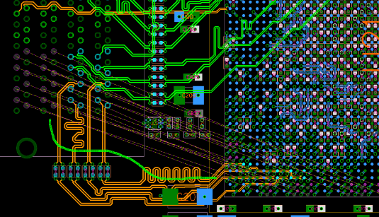
5. Managing Layers Effectively
Multi-layer PCBs require careful layer management:
- Use a Consistent Layer Stackup: Define power, ground, and signal layers clearly.
- Minimize Via Count: Excessive vias can increase cost and reduce reliability.
- Use Blind/Buried Vias for High-Density Designs: Helps in complex layouts but increases cost.
6. Creating and Using Custom Libraries
Building a personal component library saves time in future projects:
- Standardize Footprints: Ensure consistent pad sizes and silkscreen markings.
- Include 3D Models: Helps in mechanical integration (e.g., enclosure fitting).
- Verify Library Parts: Incorrect footprints can lead to assembly issues.
7. Automating Repetitive Tasks
Many PCB tools support scripting (e.g., Python in KiCad, VB in Altium) to automate tasks like:
- Bulk Renaming Components
- Generating Custom Reports
- Batch Importing/Exporting Designs
8. Generating Accurate Manufacturing Files
Before sending your design for fabrication, export the correct files:
- Gerber Files (RS-274X): Contains layer information.
- NC Drill Files: For hole drilling.
- Bill of Materials (BOM): For component procurement.
- Pick-and-Place Files: For automated assembly.
Double-check these files using a Gerber viewer like Gerbv or CAM350.
9. Collaborating with Team Members
For team projects, use version control (e.g., Git) and cloud-based collaboration tools:
- Altium 365: Cloud-based project sharing.
- KiCad + Git: Track design changes.
- Eagle + Fusion 360: Cloud integration for collaborative work.
10. Staying Updated with Software Features
PCB tools frequently release updates with new features:
- Follow Official Blogs & Forums: Learn about new tools and shortcuts.
- Watch Tutorials: Platforms like YouTube and Udemy offer advanced tips.
- Join User Communities: Exchange knowledge with other designers.
Conclusion
Mastering PCB design software involves learning shortcuts, optimizing component placement, efficient routing, and leveraging automation. By implementing these tips, you can enhance productivity, reduce errors, and produce high-quality PCB designs. Whether you’re designing simple prototypes or complex multi-layer boards, continuous learning and practice will help you become more proficient in PCB design.
Would you like a more detailed breakdown of any specific software? Let me know how I can refine this guide further!