Expert Multi-Layer PCB Manufacturing: Quality Process Guide

Key Takeaways
When evaluating PCB manufacturing options, understanding core principles ensures you select partners aligned with your project’s technical and budgetary needs. Reputable PCB manufacturing companies prioritize traceable material sourcing and automated optical inspection (AOI), which minimize defects in complex multilayer designs. A typical 33-step process spans from laser-drilled microvias to controlled impedance testing, balancing PCB manufacturing cost with performance requirements.
Tip: Always verify if your supplier adheres to IPC-6012 Class 3 standards for high-reliability applications—this reduces long-term risks in critical industries like aerospace or medical devices.
Ensuring reliability hinges on thermal stress testing and cross-sectional analysis, which identify weaknesses in layer bonding or plating. For PCB manufacturing business leaders, optimizing workflows—like adopting design-for-manufacturing (DFM) checks—can slash prototyping cycles by up to 30%. Advanced techniques such as sequential lamination or embedded passives further enhance density without compromising signal integrity.
To manage PCB manufacturing cost, consider panel utilization rates and material alternatives early in the design phase. Certified partners, like those with proven multilayer expertise, often provide real-time yield analytics to refine production efficiency. By aligning your priorities with industry-leading practices, you mitigate risks while achieving scalable, high-performance solutions.
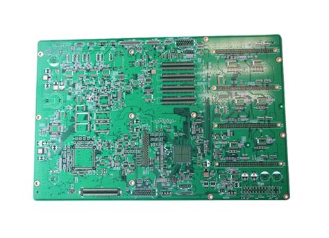
Multi-Layer PCB Manufacturing Essentials
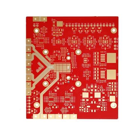
Understanding the core principles of PCB manufacturing is critical when working with multi-layer designs. Unlike single-layer boards, multi-layer PCBs require precise alignment of conductive layers, dielectric materials, and via structures to ensure signal integrity and thermal stability. Leading PCB manufacturing companies prioritize advanced lamination techniques and laser-drilled microvias to minimize layer misalignment—a common challenge that impacts both performance and PCB manufacturing cost.
When planning your design, consider how material selection (e.g., high-Tg FR4 or polyimide) affects thermal management and signal loss. These choices directly influence production complexity, which can escalate costs if not optimized early. For instance, incorporating blind or buried vias adds value to high-density designs but requires tighter tolerances during fabrication. Reputable manufacturers balance these technical demands with cost-efficiency by leveraging automated optical inspection (AOI) and controlled impedance testing.
Finally, collaboration between design teams and PCB manufacturing business experts ensures manufacturability. By addressing potential issues like copper balancing or stack-up symmetry upfront, you reduce rework risks and delays—key factors in maintaining competitive PCB manufacturing timelines. This proactive approach aligns with industry standards while safeguarding reliability across applications, from consumer electronics to aerospace systems.
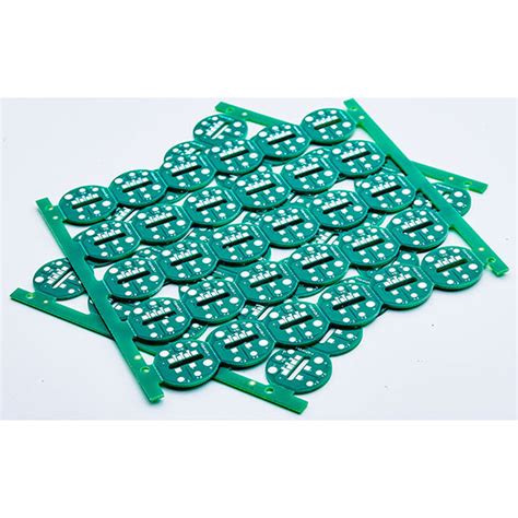
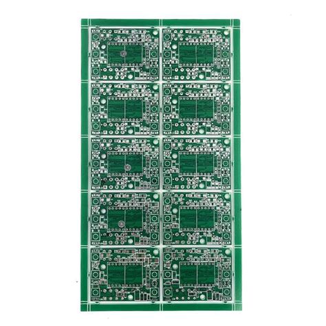
33-Step Precision PCB Process Breakdown
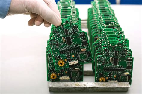
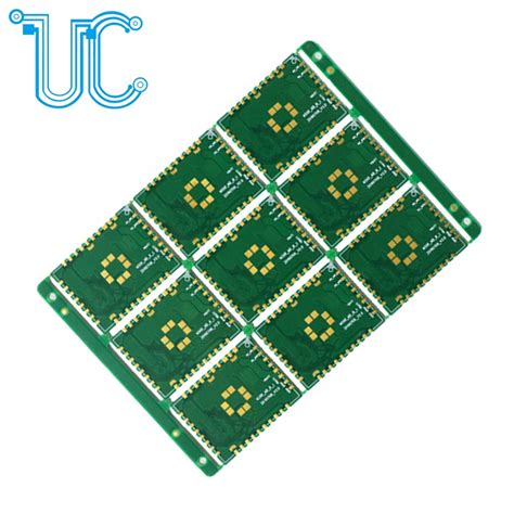
When working with PCB manufacturing companies, understanding the intricacies of their production workflow ensures you can optimize designs for both performance and PCB manufacturing cost. A typical 33-step precision process begins with design validation and material selection, where substrate quality directly impacts durability. Layers are then aligned using laser-guided systems to minimize misregistration—a critical factor in multilayer PCB manufacturing.
The core stages involve pattern etching, drilling micro-vias, and electroplating to establish interlayer connections. Automated optical inspection (AOI) follows each step, ensuring defects are caught early, reducing waste in the PCB manufacturing business. Advanced plasma desmear techniques clean drilled holes, while sequential lamination bonds layers under controlled heat and pressure.
Post-etching, solder mask application and surface finishing protect circuits from environmental stressors. Final electrical testing, including impedance checks and continuity scans, validates signal integrity. Reputable PCB manufacturing partners integrate these steps with ISO-certified protocols, balancing precision with scalability. By aligning your design specifications with this structured approach, you ensure reliability without compromising on turnaround times—key for industries demanding industry-leading production standards.
Quality Assurance in PCB Fabrication
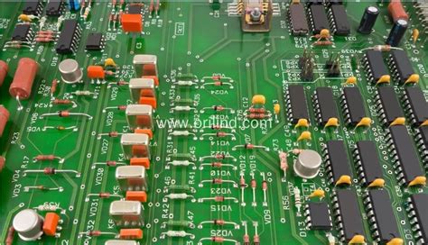
When selecting PCB manufacturing companies, understanding their approach to quality assurance (QA) ensures your multilayer boards meet exacting standards. Modern PCB manufacturing workflows incorporate automated optical inspection (AOI), electrical testing, and cross-sectional analysis to verify layer alignment, trace integrity, and material consistency. These steps minimize defects that could escalate PCB manufacturing cost through rework or recalls.
Leading manufacturers deploy statistical process control (SPC) to monitor critical parameters like copper thickness and dielectric spacing across production batches. This data-driven approach not only enhances reliability but also streamlines PCB manufacturing business operations by reducing waste. For multilayer designs, impedance testing and thermal stress simulations become vital, as even minor deviations can compromise signal integrity in high-frequency applications.
Certifications like ISO 9001 and IPC Class 3 further validate a supplier’s commitment to precision. By prioritizing QA protocols, you mitigate risks while ensuring compliance with industry benchmarks—whether prototyping or scaling production. Remember, rigorous quality checks don’t just safeguard performance; they protect your project timelines and long-term partnerships.
Ensuring Reliability in Multilayer PCBs
When selecting PCB manufacturing companies for multilayer boards, reliability hinges on rigorous process controls and material integrity. You’ll want suppliers that implement automated optical inspection (AOI) and electrical testing at critical stages to identify defects like micro-cracks or misaligned vias. These steps ensure signal integrity across layers, especially in high-density designs where PCB manufacturing cost often correlates with precision tolerances.
| Key Reliability Factor | Impact on Performance |
|---|---|
| Material Selection (e.g., FR-4, high-Tg) | Thermal stability & signal loss reduction |
| Layer Alignment Precision | Prevents impedance mismatches |
| Surface Finish (ENIG, HASL) | Enhances solderability & corrosion resistance |
For PCB manufacturing to deliver durable boards, thermal stress testing and accelerated aging simulations are non-negotiable. These protocols validate performance under extreme temperatures or humidity, critical for aerospace or automotive applications. While balancing PCB manufacturing business priorities like lead times and budgets, never compromise on certifications like ISO 9001 or IPC Class 3—they signal adherence to industry benchmarks for traceability and consistency.
Finally, collaborate with partners who optimize PCB manufacturing cost without cutting corners. Advanced techniques like laser drilling or sequential lamination might raise initial expenses but reduce field failures, ensuring long-term ROI. Always verify that your supplier’s quality reports align with your design’s operational demands.
Advanced Techniques for PCB Production
To stay competitive in modern PCB manufacturing, companies adopt advanced methodologies that balance precision, efficiency, and cost-effectiveness. High-density interconnect (HDI) technology, for instance, enables tighter trace spacing and microvia drilling, critical for compact multilayer designs. Laser direct imaging (LDI) further enhances accuracy by eliminating photomasks, reducing errors in complex layouts. When evaluating PCB manufacturing companies, prioritize those using automated optical inspection (AOI) systems, which detect defects at micron-level resolutions during production.
Another breakthrough lies in sequential lamination processes, where layers are bonded incrementally to minimize thermal stress—a key factor in PCB manufacturing cost optimization. Advanced materials like low-loss dielectrics or high-temperature laminates also improve signal integrity and durability, especially for high-frequency applications. For PCB manufacturing business models targeting industries like aerospace or medical devices, integrating impedance control testing ensures consistent performance under extreme conditions.
By aligning these techniques with lean manufacturing principles, you reduce waste while maintaining scalability. Whether refining existing workflows or adopting new technologies, the goal remains clear: deliver reliable multilayer PCBs that meet evolving industry demands without compromising on quality.
Certified PCB Manufacturing Standards
When evaluating PCB manufacturing companies, understanding their adherence to certified standards is critical for ensuring consistent quality. Reputable manufacturers comply with globally recognized frameworks like ISO 9001 and IPC-A-600, which govern everything from material selection to final inspection. These certifications validate that a PCB manufacturing business maintains rigorous documentation, process controls, and defect prevention protocols, directly influencing PCB manufacturing cost efficiency and long-term reliability.
Certified facilities prioritize traceability, using digitized systems to track each layer’s alignment, etching, and lamination. This minimizes errors in multi-layer PCB manufacturing, where even micron-level deviations can compromise performance. Independent audits further ensure compliance with environmental regulations (e.g., RoHS) and performance benchmarks, reducing risks of field failures.
For your projects, partnering with certified PCB manufacturing providers guarantees access to advanced testing equipment—such as automated optical inspection (AOI) and impedance control tools—that uphold industry-leading tolerances. By aligning with these standards, you mitigate supply chain disruptions and ensure designs meet exacting technical specifications without inflating PCB manufacturing cost unnecessarily.
Optimizing Multilayer PCB Design Workflows
When refining PCB manufacturing workflows, prioritizing design optimization ensures seamless translation from concept to production. Start by collaborating with experienced PCB manufacturing companies early in the design phase to identify potential bottlenecks. Layer stackup planning, for instance, directly impacts signal integrity and thermal management—key factors in minimizing PCB manufacturing cost while maintaining performance.
Adopting advanced simulation tools allows you to validate impedance control and via placement before prototyping, reducing iterative revisions. Integrating design-for-manufacturability (DFM) checks ensures compatibility with fabrication processes, such as precise drill alignment for high-density interconnects. This approach not only accelerates timelines but also aligns with the operational efficiencies critical for scaling a PCB manufacturing business.
Balancing performance requirements with cost constraints requires strategic material selection. For example, opting for mid-loss laminates over high-frequency alternatives can lower expenses without compromising functionality in many applications. By embedding these practices into your workflow, you create a foundation for reliability and scalability—two pillars that define competitive PCB manufacturing outcomes.
Industry-Leading PCB Production Practices
When selecting PCB manufacturing companies, you want partners that prioritize precision and scalability. Leading producers integrate automated optical inspection (AOI) systems to detect microscopic defects in real time, ensuring PCB manufacturing processes maintain <1% error rates even in high-volume runs. These practices directly impact PCB manufacturing cost by minimizing material waste and reducing post-production rework—critical factors for balancing affordability with performance.
Advanced manufacturers also adopt sequential lamination techniques for multilayer boards, combining controlled impedance testing with thermal stress simulations. This approach addresses signal integrity challenges while enhancing durability, a key differentiator in competitive PCB manufacturing business environments. By leveraging laser-direct imaging (LDI) for finer trace resolutions, top-tier facilities achieve 25µm line widths—essential for high-density interconnect (HDI) designs.
You’ll notice industry leaders emphasize traceability through blockchain-enabled supply chain tracking, ensuring every material complies with RoHS and IPC-6012 standards. This aligns with their focus on preventive quality control rather than reactive fixes, a strategy proven to reduce failure rates by 40% in field applications. When optimizing your projects, prioritize partners offering design-for-manufacturability (DFM) consultations—this collaboration bridges prototyping and mass production while controlling PCB manufacturing cost through early error detection.
Conclusion
When selecting a PCB manufacturing partner, understanding the interplay between quality, cost, and reliability becomes critical. Reputable PCB manufacturing companies prioritize rigorous process controls—such as the 33-step precision workflow—to minimize defects and ensure compliance with international standards. While PCB manufacturing cost may vary based on design complexity and material choices, investing in certified providers safeguards against costly rework or field failures. For businesses scaling their PCB manufacturing business, adopting advanced techniques like automated optical inspection (AOI) and impedance testing ensures consistent output, even for high-layer-count designs.
Ultimately, the success of your project hinges on aligning with manufacturers that balance technical expertise with transparent communication. By prioritizing traceability in material sourcing and data-driven quality assurance, you mitigate risks while achieving performance targets. Whether prototyping or transitioning to mass production, partnering with ISO-certified PCB manufacturing specialists guarantees adherence to industry-leading standards and positions your product for long-term reliability in demanding applications.
FAQs
How do you choose the right PCB manufacturing partner for multilayer designs?
Look for PCB manufacturing companies with certifications like ISO 9001 and IPC-A-600. Verify their expertise in handling high-density interconnects and thermal management—critical for multilayer boards.
What factors influence PCB manufacturing cost for multilayer projects?
Cost depends on layer count, material selection (e.g., FR-4 vs. high-frequency laminates), and precision requirements. Partnering with experienced PCB manufacturing providers ensures cost efficiency without compromising quality.
How do manufacturers ensure reliability in multilayer PCBs?
Reliability stems from automated optical inspection (AOI), electrical testing, and adherence to industry-leading production standards. Reputable PCB manufacturing businesses also perform thermal cycling tests to validate durability.
Can design choices impact the success of a PCB manufacturing project?
Absolutely. Optimizing trace routing and stack-up configuration reduces signal loss. Collaborate early with your manufacturer to align design workflows with their advanced fabrication techniques.
Why are certifications critical in PCB manufacturing?
Certifications like UL listing or RoHS compliance validate adherence to safety and environmental standards. They signal a manufacturer’s commitment to quality assurance, crucial for aerospace or medical applications.
Ready to Start Your Multilayer PCB Project?
For expert guidance and a 33-step precision manufacturing process, click here to connect with certified professionals. Ensure your next project meets industry-leading benchmarks for performance and reliability.