Expert OEM PCB Manufacturer Processes for Quality Assembly
Key Takeaways
When selecting an PCB manufacturing partner, understanding their adherence to IPC standards ensures your boards meet global quality benchmarks. Top PCB manufacturing companies integrate automated optical inspection (AOI) and functional testing to eliminate defects in multi-layer designs. For instance, optimizing layer stack-ups and via placement reduces signal loss, which is critical for high-frequency applications.
"Investing in a manufacturer with ISO 9001 certification guarantees traceability across every production stage—essential for aerospace or medical-grade PCB assemblies."
Here’s a breakdown of factors influencing PCB manufacturing cost:
| Cost Driver | Impact Level | Optimization Strategy |
|---|---|---|
| Layer Complexity | High | Simplify stack-up where possible |
| Material Selection | Moderate | Use FR-4 instead of high-frequency substrates |
| Order Volume | High | Leverage bulk pricing discounts |
| Turnaround Time | Moderate | Plan ahead to avoid rush fees |
Balancing cost-efficiency with performance requires aligning your PCB manufacturing business goals with scalable solutions. For example, heavy copper boards (3 oz+) demand specialized etching but enhance thermal management in power electronics. Meanwhile, advanced SMT lines with 01005 component placement capabilities future-proof your designs without inflating budgets.
Pro Tip:
"Always request a Design for Manufacturability (DFM) report—it identifies potential flaws in Gerber files before production, saving weeks of revisions."
If you’re comparing OEM and ODM models, prioritize suppliers offering flexible NPI (New Product Introduction) support. This ensures smoother transitions from prototyping to mass production while maintaining PCB manufacturing consistency across batches.
IPC Standards for Quality PCB Assembly
When selecting an OEM PCB manufacturer, understanding their adherence to IPC standards is critical for ensuring consistent quality. These globally recognized guidelines govern everything from material selection to final inspection, directly impacting the reliability of your pcb manufacturing outcomes. For instance, IPC-A-600 outlines acceptability criteria for printed boards, while IPC-6012 defines performance requirements for rigid circuit boards. Manufacturers certified in these standards minimize defects like soldering voids or misaligned layers, which can escalate pcb manufacturing cost over time.
Leading pcb manufacturing companies integrate IPC protocols into their workflows through automated optical inspection (AOI) and in-circuit testing (ICT). These steps verify compliance with Class 2 (commercial electronics) or Class 3 (high-reliability systems) specifications, depending on your product’s end use. By prioritizing traceability and documentation, they ensure that deviations are flagged early—reducing rework expenses and maintaining project timelines.
Cost efficiency in the pcb manufacturing business isn’t just about lowering upfront prices—it’s about avoiding post-production failures. IPC-2221, for example, dictates design rules for thermal management and spacing, preventing issues like solder joint fatigue. Partnering with a manufacturer that rigorously applies these standards helps you sidestep field returns or warranty claims, which can erode profit margins.
Transitioning to advanced processes like surface-mount technology (SMT) or multilayer builds becomes smoother when IPC frameworks guide material compatibility and assembly techniques. This alignment ensures that your boards meet both functional requirements and industry certifications, whether for consumer electronics or aerospace applications. By embedding these standards into their quality systems, manufacturers create a foundation for scalable, repeatable production—key for OEMs balancing innovation with risk mitigation.
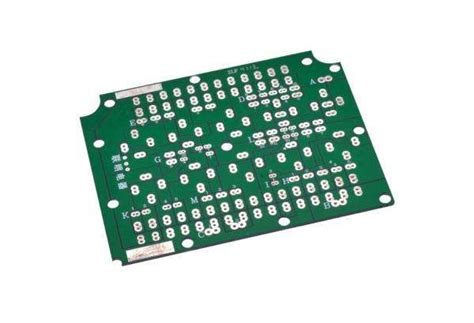
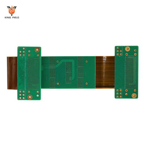
Multi-Layer Board Design Optimization Tips
When designing multi-layer boards for PCB manufacturing, balancing performance and pcb manufacturing cost requires strategic planning. Start by optimizing your layer stack-up configuration. Properly arranging signal, ground, and power layers minimizes electromagnetic interference (EMI) and enhances signal integrity—critical for high-speed or RF applications. For instance, placing ground planes adjacent to signal layers reduces crosstalk, ensuring consistent performance in dense layouts.
Material selection also plays a pivotal role. High-frequency applications demand low-loss substrates like Rogers or Isola, while standard FR-4 suffices for cost-sensitive projects. Partnering with experienced pcb manufacturing companies ensures access to material databases and design-for-manufacturability (DFM) feedback, preventing costly revisions. For example, adjusting trace widths based on copper weight and dielectric properties avoids impedance mismatches, a common pitfall in multi-layer designs.
Thermal management is another key consideration. Integrating thermal vias near high-power components dissipates heat efficiently, preventing hotspots that degrade reliability. This becomes especially vital in designs combining heavy copper layers with fine-pitch components.
To streamline your pcb manufacturing business workflows, leverage automated design tools for via placement and routing. Advanced software can simulate signal behavior and thermal dynamics, allowing you to refine layouts before prototyping. However, always validate designs with your manufacturer early—subtle factors like solder mask application or plating thickness can impact yield rates.
Finally, align your design choices with scalable production processes. For example, standardizing hole sizes and panelization strategies reduces setup times and material waste. By prioritizing these optimizations, you achieve a balance between performance, durability, and cost—factors that define success in competitive PCB manufacturing landscapes. For tailored solutions, explore how industry leaders integrate these principles into their production frameworks.
Cost-Efficient OEM Manufacturing Solutions
When optimizing PCB manufacturing processes for cost efficiency, it’s critical to balance economies of scale with precision engineering. Leading PCB manufacturing companies achieve this by streamlining material sourcing, leveraging advanced fabrication technologies, and implementing strategic design-for-manufacturability (DFM) principles. For instance, consolidating orders or standardizing component libraries reduces PCB manufacturing cost by minimizing material waste and setup redundancies.
A key driver of affordability lies in smart panelization strategies. By grouping multiple board designs into a single production panel, manufacturers maximize substrate utilization—directly lowering per-unit expenses. This approach is particularly impactful for high-volume orders, where even marginal savings per board compound significantly. However, cost-cutting never compromises quality: reputable providers adhere to IPC-6012 standards for material integrity and layer alignment, ensuring reliability across applications.
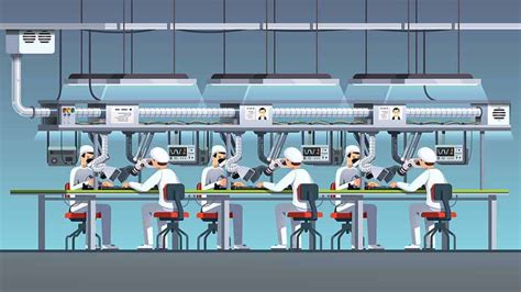
Automation plays a pivotal role in modern PCB manufacturing business models. Robotic assembly lines with AI-driven optical inspection (AOI) systems slash labor costs while maintaining defect rates below 0.1%. Additionally, partnering with suppliers offering end-to-end services—from prototyping to testing—eliminates logistical overheads. For example, integrated surface-mount technology (SMT) lines reduce handling steps, accelerating turnaround times by up to 30%.
To further control expenses, consider modular design frameworks that allow component reuse across product lines. This reduces redesign costs and simplifies inventory management. Transparent pricing models, such as tiered volume discounts or consignment stocking agreements, also help align PCB manufacturing cost with budgetary constraints. Ultimately, the most sustainable savings emerge from collaborative partnerships where OEMs and manufacturers co-optimize designs for both performance and producibility.
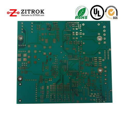
Rigorous Quality Control in PCB Production
When choosing PCB manufacturing companies, understanding their quality assurance protocols is critical to ensuring your electronic devices perform reliably. Industry-leading manufacturers implement multi-stage inspection systems that begin with raw material verification and extend through final product testing. For instance, advanced PCB manufacturing workflows integrate automated optical inspection (AOI) to detect microscopic defects in solder joints or trace alignment, while X-ray imaging validates internal layer integrity in multi-board designs.
A key differentiator among top-tier suppliers is their adherence to IPC-A-610 and IPC-6012 standards, which define acceptability criteria for PCB manufacturing business operations. These guidelines ensure consistency in hole wall thickness, copper plating uniformity, and impedance control—factors that directly impact signal integrity. By enforcing strict process capability indices (Cpk), manufacturers minimize variability, reducing PCB manufacturing cost overruns caused by rework or scrap.
Transitioning from design to production, statistical process control (SPC) tools track critical parameters like lamination pressure and etching rates. This data-driven approach allows for real-time adjustments, preventing batch failures before they occur. You’ll find that suppliers investing in flying probe testers and boundary scan diagnostics often achieve defect rates below 50 parts per million, a benchmark for aerospace and medical-grade assemblies.
To maintain competitiveness, forward-thinking PCB manufacturing partners are now incorporating artificial intelligence into their quality systems. Machine learning algorithms analyze historical failure patterns to predict and mitigate risks in new orders, creating a feedback loop that continuously refines production accuracy. Such innovations not only safeguard product reliability but also streamline compliance documentation—a crucial advantage for industries requiring full traceability.
By prioritizing these rigorous protocols, you ensure that your PCB manufacturing cost aligns with long-term value rather than short-term savings, building a foundation for electronics that withstand real-world operational stresses.
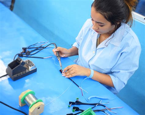
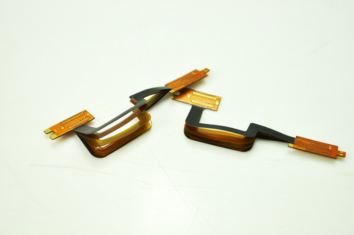
Advanced SMT Applications in PCB Assembly
When optimizing PCB manufacturing workflows, advanced Surface Mount Technology (SMT) plays a pivotal role in balancing precision, speed, and scalability. Modern high-speed pick-and-place systems enable PCB manufacturing companies to position components with micron-level accuracy, even on densely packed multi-layer boards. By integrating vision-guided robotics, these systems reduce placement errors to less than 0.01mm, ensuring compatibility with miniaturized designs common in IoT and wearable electronics.
A critical advantage of SMT lies in its ability to streamline PCB manufacturing cost structures. Automated solder paste application and reflow ovens eliminate manual soldering inefficiencies, cutting assembly time by up to 60% compared to through-hole methods. This efficiency is further amplified when producing high-volume orders, where economies of scale reduce per-unit expenses. However, achieving consistent results demands strict adherence to thermal profiles—deviations as small as 5°C during reflow can compromise solder joint integrity.
For businesses scaling their PCB manufacturing business, hybrid SMT-thru-hole configurations offer flexibility. For instance, mixed-technology boards combine surface-mounted ICs with through-hole connectors for mechanical stability, catering to industrial applications requiring vibration resistance. Advanced manufacturers also employ 3D AOI (Automated Optical Inspection) systems post-SMT to detect tombstoning or solder bridging, addressing defects before functional testing.
Transitioning to next-gen SMT solutions requires evaluating your design’s compatibility with fine-pitch components (e.g., 0.4mm BGA packages) and lead-free solder alloys. Partnering with PCB manufacturing companies that maintain IPC-A-610 Class 3 certification ensures assemblies meet rigorous aerospace or medical-grade standards. This alignment between SMT capabilities and application-specific requirements ultimately determines both product reliability and long-term production viability.
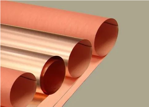
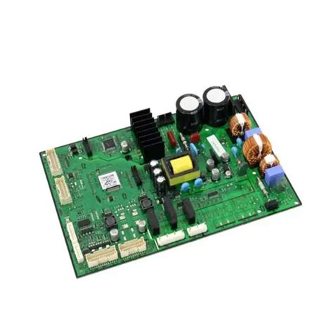
Heavy Copper Circuit Board Fabrication
When designing high-power or high-current applications, heavy copper circuit boards become indispensable. Unlike standard PCBs, these specialized boards use copper layers exceeding 3 oz/ft² (105 µm), with some pcb manufacturing companies offering up to 20 oz/ft² for extreme durability. The increased copper thickness enhances current-carrying capacity, reduces thermal strain, and improves mechanical stability—critical for industries like automotive, industrial controls, and renewable energy systems.
However, fabricating heavy copper boards demands precision engineering. Thermal management becomes paramount, as uneven heat distribution during plating can lead to zonal over-etching or delamination. Reputable pcb manufacturing partners employ modified etching techniques, such as differential plating and step-controlled deposition, to maintain trace integrity while achieving target copper weights. This technical expertise directly impacts pcb manufacturing cost, as material usage and process complexity rise with copper thickness.
For businesses balancing performance and budget, optimizing layer stack-ups proves vital. Combining heavy copper outer layers with standard inner cores can reduce pcb manufacturing business expenses by up to 18% while meeting IPC-2221A thermal requirements. Advanced manufacturers also implement hybrid designs—embedding thick copper sections only in high-stress areas—to minimize material waste.
Quality validation remains non-negotiable. Reliable suppliers conduct microsection analysis to verify copper uniformity and thermal cycle testing (up to 1,000 cycles) to assess solder joint reliability under load fluctuations. These protocols ensure your boards withstand 15–20% higher current densities than conventional alternatives without compromising longevity.
When selecting partners for heavy copper projects, prioritize pcb manufacturing companies with documented expertise in high-reliability applications. Their ability to harmonize material selection, fabrication techniques, and testing rigor will determine both your product’s performance and long-term pcb manufacturing cost efficiency.
OEM vs ODM Manufacturing Considerations
When evaluating partnerships for PCB manufacturing, understanding the distinction between OEM (Original Equipment Manufacturing) and ODM (Original Design Manufacturing) is critical. While PCB manufacturing companies often offer both services, your choice hinges on design ownership, prototyping timelines, and control over pcb manufacturing cost structures.
With OEM, you retain full intellectual property (IP) rights to your board designs, allowing tighter oversight of material selection and production workflows. This approach suits businesses requiring specialized pcb manufacturing business models or proprietary technologies. However, it demands higher upfront investments in design validation and tooling. In contrast, ODM leverages pre-engineered solutions from manufacturers, accelerating time-to-market but limiting customization. This trade-off often reduces per-unit pcb manufacturing cost for standardized projects, though it may compromise differentiation in competitive markets.
Balancing these factors requires assessing your technical capabilities and market goals. For instance, startups with limited R&D resources might prioritize ODM to minimize risks, while established enterprises often opt for OEM to safeguard IP and optimize performance. Always verify whether potential partners align with IPC-A-610 or ISO 9001 benchmarks, as rigorous quality frameworks apply equally to both models. Transparent communication about testing protocols, scalability, and post-production support ensures alignment with your pcb manufacturing objectives—whether you’re iterating prototypes or scaling high-volume orders.
Conclusion
When selecting an OEM PCB manufacturer, it’s essential to prioritize partners that align with your technical and operational requirements. Leading PCB manufacturing companies distinguish themselves by balancing precision engineering with scalable solutions, ensuring your designs transition seamlessly from prototype to mass production. A critical factor in this process is understanding how PCB manufacturing cost structures impact your bottom line—whether through material selection, layer optimization, or advanced assembly techniques.
For businesses in the PCB manufacturing business, maintaining compliance with IPC-6012 and IPC-A-610 standards isn’t just a formality—it’s a foundation for reliability. Rigorous testing protocols, including automated optical inspection (AOI) and functional testing, safeguard against defects that could compromise end-product performance. Equally critical is leveraging design-for-manufacturability (DFM) principles to minimize waste and streamline production timelines.
Additionally, modern PCB manufacturing demands adaptability. Whether your project requires high-density interconnect (HDI) layouts, heavy copper substrates, or mixed-technology assembly, partnering with a manufacturer that offers end-to-end solutions ensures consistency across every batch. Cost efficiency doesn’t mean cutting corners; it’s achieved through intelligent material sourcing, process automation, and economies of scale.
Ultimately, the success of your electronics hinges on collaboration. Transparent communication with your PCB manufacturing partner about timelines, certifications, and risk mitigation strategies fosters long-term trust. By aligning your goals with a manufacturer’s technical expertise, you secure not just components, but a competitive edge in an evolving market.
FAQs
How do you choose reliable PCB manufacturing companies for OEM projects?
Look for PCB manufacturing partners certified under IPC-A-610 and IPC-6012 standards, which validate adherence to quality assembly processes. Assess their expertise in multi-layer designs, heavy copper fabrication, and SMT applications to ensure compatibility with your project’s technical demands.
What factors influence PCB manufacturing cost in OEM production?
Cost depends on board complexity, material selection (e.g., high-frequency laminates), layer count, and volume. Optimizing designs for DFM principles and partnering with PCB manufacturing businesses offering scalable solutions can reduce expenses without compromising performance.
Why opt for OEM over ODM in PCB manufacturing?
OEM services allow full control over design and specifications, ideal for proprietary projects. In contrast, ODM relies on the manufacturer’s pre-existing designs. For tailored solutions requiring rigorous quality control, OEM partnerships are often preferable.
How do PCB manufacturing companies ensure quality consistency?
Reputable providers implement automated optical inspection (AOI), X-ray testing, and functional testing aligned with IPC standards. Regular audits and traceability systems further guarantee reliability across high-volume orders.
Can you reduce PCB manufacturing cost without sacrificing quality?
Yes. Simplify layouts, standardize materials, and leverage economies of scale. Many PCB manufacturing businesses offer cost-sharing programs for prototype batches or long-term contracts, balancing affordability and precision.
What makes heavy copper PCBs unique in PCB manufacturing?
With copper weights exceeding 3 oz, these boards excel in high-power and thermal applications. They require specialized etching and plating techniques, so verify your manufacturer’s expertise in heavy copper fabrication for optimal durability.
How critical are SMT applications in modern PCB assembly?
SMT enables smaller, faster, and more reliable boards by mounting components directly onto surfaces. Ensure your PCB manufacturing partner uses advanced pick-and-place machines and reflow ovens to maintain precision in high-density designs.
What turnaround times can you expect from PCB manufacturing companies?
Lead times vary from 24 hours for prototypes to 2–3 weeks for complex multi-layer orders. Prioritize suppliers with transparent scheduling and rush-order options to align with your project timeline.
Ready to Streamline Your PCB Production?
For tailored PCB manufacturing solutions that balance quality and affordability, please click here to explore advanced engineering support and instant quoting tools.