Expert PCB Prototyping: Rapid Fabrication Techniques

Key Takeaways
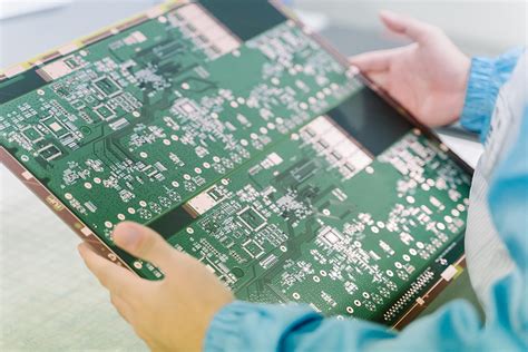
When navigating PCB manufacturing for prototypes, understanding core efficiency drivers ensures you avoid costly delays. Leading PCB manufacturing companies leverage advanced techniques like automated optical inspection (AOI) and direct laser imaging (DLI) to achieve 24-hour build times without compromising precision. For low-volume projects, optimizing PCB manufacturing cost often hinges on material selection and panel sharing—grouping multiple designs into a single panel to reduce waste.
Tip: Always verify if your provider offers dynamic panelization—this can lower expenses by up to 30% in low-volume PCB assembly.
Instant quoting tools streamline budgeting, allowing you to compare PCB manufacturing business pricing tiers transparently. Precision SMT stencils, critical for accurate solder paste application, are often included in prototyping packages to ensure repeatability. For global teams, partnering with manufacturers offering regional fulfillment hubs minimizes shipping delays—a key advantage when scaling production.
Transitioning from prototype to mass production? Evaluate providers with integrated supply chains to maintain consistency. While speed is vital, prioritize vendors with ISO-certified workflows to mitigate risks in fast-turn PCB production. By balancing urgency with quality checks, you safeguard your design’s integrity across every iteration.
Rapid PCB Prototyping Techniques Explained
When developing electronic products, speed and precision in PCB manufacturing are critical. Modern PCB manufacturing companies leverage advanced techniques to accelerate prototyping while maintaining quality. For instance, automated routing algorithms reduce design-to-production time, enabling engineers to iterate designs within hours. Pairing this with laser direct imaging (LDI) ensures tighter tolerances for high-density circuits, a necessity for complex prototypes.
One key consideration is balancing PCB manufacturing cost with turnaround speed. Techniques like panel sharing—grouping multiple designs on a single board—optimize material usage, cutting expenses by up to 30%. Additive printing methods, such as inkjet deposition of conductive traces, further minimize waste compared to traditional subtractive processes. Below is a comparison of common rapid prototyping methods:
| Technique | Speed | Cost Efficiency | Best For |
|---|---|---|---|
| LDI | 12-24 hours | Moderate | High-precision designs |
| Additive Printing | 24-48 hours | High | Low-volume batches |
| Automated Routing | 6-12 hours | Low | Iterative revisions |
To sustain a competitive PCB manufacturing business, adopting these methods ensures you meet client demands for both speed and affordability. Real-time design validation tools further streamline workflows, allowing immediate adjustments before production. By integrating these strategies, you reduce risks of delays while maintaining control over PCB manufacturing cost, paving the way for scalable prototyping solutions.
24-Hour Build Times for PCB Fabrication
When accelerating product development, PCB manufacturing companies leverage advanced workflows to deliver functional prototypes within 24 hours. This rapid turnaround hinges on automated design validation, high-speed milling, and direct laser imaging systems that eliminate traditional bottlenecks. By optimizing material preparation and layer alignment, these providers minimize PCB manufacturing cost while maintaining tight tolerances—critical for testing complex designs under real-world conditions.
You’ll find that streamlined order processing plays a key role here. Reputable firms integrate instant quoting tools to analyze your Gerber files, layer count, and material specs in minutes, ensuring no delays before production begins. For low-volume projects, panel sharing further reduces expenses by grouping multiple designs onto a single board. However, speed doesn’t compromise quality: automated optical inspection (AOI) and electrical testing verify functionality even in accelerated timelines.
For PCB manufacturing business clients, 24-hour builds mean faster iterations—whether refining IoT sensors or medical devices. Global logistics networks then ensure overnight shipping, compressing the entire cycle from concept to validation. This approach aligns with lean product development strategies, letting you test ideas rapidly without inflating budgets.
Low-Volume PCB Assembly Cost Efficiency
When managing PCB manufacturing for small batches, balancing speed and affordability requires strategic planning. Unlike high-volume production, low-volume assembly leverages specialized workflows to minimize PCB manufacturing cost without compromising quality. By partnering with PCB manufacturing companies that prioritize flexible order sizes, you avoid overstocking or underutilizing materials—a common pain point in the PCB manufacturing business.
Key cost-saving measures include design optimization (e.g., reducing layer counts or standardizing component sizes) and panelization strategies that maximize material usage. Advanced providers often integrate automated DFM (Design for Manufacturability) checks to flag inefficiencies early, preventing costly revisions. For prototypes or niche products, shared panel programs allow you to split fabrication costs with other projects, further lowering per-unit expenses.
Additionally, modular pricing models let you scale orders precisely, paying only for the components and labor you need. This approach aligns with lean manufacturing principles, ensuring your PCB manufacturing cost remains predictable even for complex designs. By selecting partners with transparent quoting tools and global supply chains, you gain access to competitive pricing while maintaining rapid turnaround times—critical for iterative development cycles.
Transitioning to the next section, precision in PCB manufacturing extends beyond assembly efficiency, particularly when leveraging specialized tools like SMT stencils.
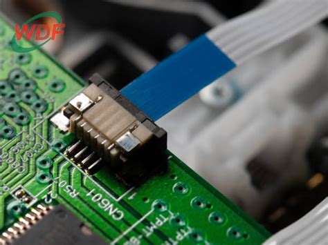
Precision SMT Stencils in Prototyping
When accelerating PCB manufacturing timelines, the role of precision SMT stencils becomes critical. These stencils ensure accurate solder paste application, directly impacting the reliability of surface-mount components during prototyping. Leading PCB manufacturing companies leverage laser-cut stainless steel stencils with ±0.02mm tolerance to eliminate misalignment risks, even in high-density designs. By investing in advanced stencil fabrication, you reduce rework and avoid costly delays—key factors in managing PCB manufacturing cost for low-volume projects.
Material selection also plays a role: electroformed nickel stencils offer durability for repeated use, while nano-coated variants prevent solder paste adhesion issues. When evaluating PCB manufacturing business partners, verify their stencil capabilities alongside prototyping services. This ensures consistency across design iterations and maintains alignment with automated assembly workflows. Transitioning seamlessly to instant quoting, these precision tools streamline your path from prototype validation to scalable production.
Instant Quoting for PCB Fabrication Services
Modern PCB manufacturing workflows prioritize efficiency, and instant quoting systems have become essential for streamlining project planning. When you request a quote online, advanced algorithms analyze your design files, layer counts, material preferences, and turnaround needs to generate real-time pricing. This transparency eliminates guesswork around PCB manufacturing cost, allowing you to compare options from multiple PCB manufacturing companies without delays. Leading providers integrate these tools directly into their platforms, factoring in variables like copper weight, surface finishes, and panelization requirements.
By automating cost estimation, PCB manufacturing business models reduce administrative overhead, passing savings to clients. You’ll often see breakdowns for prototyping phases—such as drilling, etching, and testing—helping you identify areas to optimize budgets. For low-volume orders, instant quotes account for economies of scale, ensuring you don’t overpay for small batches. Some systems even adjust pricing dynamically if you relax tolerances or extend lead times.
To maximize value, ensure your design files adhere to the manufacturer’s guidelines—incorrect formats or missing layers can skew estimates. Reputable platforms also offer live support to clarify technical requirements before finalizing orders. With instant quoting, you gain control over timelines and expenses, making it easier to align prototyping phases with broader project goals.
Global Delivery Solutions for PCB Orders
When sourcing PCB manufacturing services, global reach becomes critical for scaling your operations or maintaining supply chain resilience. Leading PCB manufacturing companies now offer integrated logistics networks that ensure components reach your doorstep—whether you’re in Silicon Valley or Singapore—within guaranteed timelines. These providers optimize shipping routes and leverage regional distribution hubs to minimize delays, a key factor when managing tight production schedules.
Cost efficiency remains central to international logistics. By negotiating bulk freight rates and streamlining customs documentation, top-tier suppliers reduce PCB manufacturing cost overheads for cross-border orders. You’ll find options like air freight for urgent prototypes or sea freight for low-volume bulk shipments, allowing flexibility based on project timelines. Modern providers also integrate real-time tracking systems, so you can monitor shipments as they move through complex global channels.
For businesses building a PCB manufacturing business, selecting partners with proven international expertise ensures compliance with regional regulations, from RoHS in Europe to FCC standards in the Americas. Strategic partnerships with logistics specialists further mitigate risks like customs hold-ups or last-mile delivery challenges. By aligning with providers that prioritize both speed and reliability, you maintain continuity in product development cycles while expanding market reach.
Optimizing Prototyping With Panel Sharing
When prototyping PCBs, panel sharing offers a strategic way to reduce pcb manufacturing cost while maintaining quality. This approach involves combining multiple designs onto a single production panel, maximizing material utilization and minimizing waste. Batch processing becomes more efficient as pcb manufacturing companies can fabricate several prototypes in parallel, lowering per-unit expenses. For your pcb manufacturing business, this method is particularly valuable for low-volume orders, where tooling fees might otherwise dominate costs.
By collaborating with manufacturers that support panelization, you gain flexibility in scaling prototypes without compromising turnaround times. Most pcb manufacturing providers offer automated panel design tools to ensure proper spacing and alignment, reducing errors during depaneling. However, always verify design rules—such as clearances and fiducial markers—to avoid complications during assembly.
This optimization also benefits pcb manufacturing cost structures for clients requiring iterative testing. Sharing panel space with other projects distributes fixed expenses, making small-batch prototyping economically viable. Additionally, material utilization improvements align with sustainable practices, appealing to eco-conscious partners. While panel sharing accelerates production, ensure your manufacturer maintains rigorous quality checks to prevent cross-project contamination or defects. This balance of speed and precision is key to refining designs efficiently.
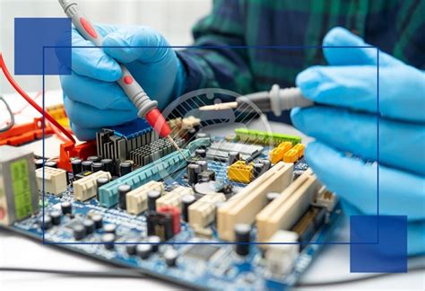
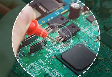
Ensuring Quality in Fast-Turn PCB Production
When accelerating production timelines, maintaining quality becomes critical in PCB manufacturing. Leading PCB manufacturing companies implement multi-stage verification processes, combining automated optical inspection (AOI) with X-ray testing to detect micro-defects in high-density designs. You’ll find that rigorous testing protocols offset risks associated with rapid fabrication, ensuring even 24-hour builds meet IPC Class 2/3 standards.
To balance speed and precision, suppliers optimize PCB manufacturing cost by leveraging advanced CAM software for real-time error correction. This minimizes material waste while preserving signal integrity in complex layouts. For low-volume orders, statistical process control (SPC) tracks critical parameters like copper thickness and solder mask alignment, preventing batch inconsistencies.
In fast-turn PCB manufacturing business models, material selection plays a pivotal role. Trusted partners use certified substrates and solder masks from vetted suppliers, reducing thermal expansion mismatches during assembly. Additionally, they provide detailed DFM reports to refine your design before fabrication, avoiding delays from iterative revisions.
By prioritizing traceability and compliance (ISO 9001, UL certification), reliable manufacturers ensure your prototypes transition seamlessly to mass production without sacrificing reliability—proving speed and quality aren’t mutually exclusive.
Conclusion
When navigating the complexities of PCB manufacturing, selecting the right partner among PCB manufacturing companies can determine your project’s success. Rapid fabrication techniques enable you to iterate designs faster while maintaining control over PCB manufacturing cost, ensuring your budget aligns with prototyping goals. For startups and established businesses alike, balancing speed with precision remains critical—advanced tools like laser-cut stencils and automated assembly minimize errors, even in low-volume runs.
By leveraging panel sharing and streamlined workflows, you reduce material waste and accelerate timelines, directly benefiting your PCB manufacturing business. Global delivery networks further eliminate logistical bottlenecks, allowing you to focus on refining designs rather than managing supply chains. Remember, instant quoting platforms provide transparency, helping you compare services and costs without delays.
Whether you’re validating a new concept or scaling toward production, modern PCB manufacturing solutions prioritize both agility and reliability. The right strategies not only compress development cycles but also lay the groundwork for seamless transitions to high-volume manufacturing—ensuring your innovations reach the market faster, smarter, and more cost-effectively.
FAQs
How does rapid prototyping affect PCB manufacturing cost?
Rapid techniques like 24-hour build times reduce downtime and accelerate product testing, lowering overall development expenses. By partnering with specialized PCB manufacturing companies, you gain access to cost-sharing models like panelization, which optimizes material usage for low-volume orders.
What should you prioritize when selecting a PCB manufacturing business?
Focus on certifications (e.g., ISO, UL), advanced equipment for precision SMT stencils, and transparent pricing. Reputable providers offer instant quoting tools to streamline budgeting and avoid hidden fees in PCB manufacturing workflows.
Can fast-turn services compromise quality in PCB manufacturing?
Not if the supplier implements rigorous testing protocols. Automated optical inspection (AOI) and functional testing ensure reliability, even with global delivery timelines. Always verify if the PCB manufacturing company adheres to industry standards like IPC-A-600.
How do you balance speed and low-volume PCB manufacturing cost?
Leverage panel sharing to split fabrication expenses across multiple clients. Many PCB manufacturing businesses offer this option, reducing per-unit costs while maintaining rapid turnaround for prototypes.
Ready to Start Your Project?
For tailored solutions in PCB manufacturing, please click here to explore services combining speed, affordability, and certified quality. Get an instant quote and discuss your prototyping needs today.