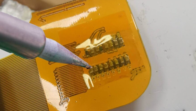
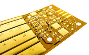
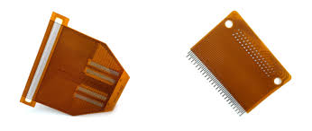
Expose copper flex pcb
Advantages Of Using Expose Copper Flex PCB In Modern Electronics
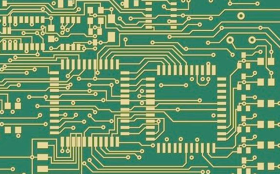
Expose copper flex PCBs, or flexible printed circuit boards, have become increasingly integral in the realm of modern electronics. These advanced components offer a multitude of advantages that cater to the evolving demands of contemporary electronic devices.
One of the primary benefits of expose copper flex PCBs is their remarkable flexibility.
Unlike traditional rigid PCBs, these flexible circuits can be bent, folded, and twisted without compromising their functionality. This adaptability is particularly advantageous in applications where space constraints and complex geometries are prevalent, such as in wearable technology, medical devices, and compact consumer electronics.
In addition to their physical flexibility, expose copper flex PCBs are known for their lightweight nature.
The reduction in weight is a critical factor in the design and development of portable electronic devices. By utilizing flexible circuits, manufacturers can produce lighter products without sacrificing performance or durability. This weight reduction also contributes to improved energy efficiency, as lighter devices typically require less power to operate, thereby extending battery life and enhancing overall user experience.
Another significant advantage of expose copper flex PCBs is their ability to withstand harsh environmental conditions.
These circuits are often designed with materials that offer superior resistance to extreme temperatures, moisture, and chemicals. This resilience makes them ideal for use in automotive, aerospace, and industrial applications, where reliability and durability are paramount. Furthermore, the robust nature of flexible PCBs ensures that they can endure repeated mechanical stress, such as bending and flexing, without experiencing failure or degradation.
The integration of expose copper flex PCBs also facilitates enhanced electrical performance.
The use of high-quality copper as the conductive material ensures excellent electrical conductivity, which is essential for maintaining signal integrity and reducing power loss. Additionally, the design flexibility of these circuits allows for optimized routing of electrical pathways, minimizing the risk of interference and crosstalk. This results in improved overall performance and reliability of the electronic device.
Moreover, expose copper flex PCBs contribute to the miniaturization of electronic devices.
As technology continues to advance, there is a growing demand for smaller, more compact products. Flexible circuits enable designers to create intricate and compact layouts that would be challenging or impossible to achieve with rigid PCBs. This capability is particularly beneficial in the development of next-generation smartphones, tablets, and other portable gadgets, where space is at a premium.
The manufacturing process of expose copper flex PCBs also offers several advantages.
These circuits can be produced using roll-to-roll processing, which is a highly efficient and cost-effective method. This technique allows for the continuous production of flexible circuits, reducing manufacturing time and costs. Additionally, the use of advanced materials and fabrication techniques ensures high precision and consistency in the final product, further enhancing the quality and reliability of the electronic devices in which they are used.
In conclusion, expose copper flex PCBs present a myriad of advantages that make them indispensable in modern electronics. Their flexibility, lightweight nature, environmental resilience, superior electrical performance, and contribution to device miniaturization are just a few of the reasons why they are increasingly favored by manufacturers and designers alike. As technology continues to evolve, the role of flexible circuits in shaping the future of electronic devices is set to become even more significant, driving innovation and enabling the development of cutting-edge products that meet the ever-changing needs of consumers and industries.
Manufacturing Process Of Expose Copper Flex PCB
The manufacturing process of expose copper flex PCBs, or flexible printed circuit boards, is a sophisticated and intricate procedure that demands precision and expertise. This process begins with the selection of appropriate materials, which typically include a flexible substrate such as polyimide or polyester. These materials are chosen for their excellent thermal stability, flexibility, and electrical insulation properties, which are crucial for the performance and durability of the final product.
Once the substrate is selected, the next step involves the application of a thin layer of copper foil onto the substrate.
This copper layer serves as the conductive material for the circuit. The copper foil is laminated onto the substrate using heat and pressure, ensuring a strong bond between the two materials. This lamination process is critical, as it ensures the integrity and reliability of the circuit during its operational life.
Following the lamination, the next phase is the application of a photoresist layer onto the copper surface.
The photoresist is a light-sensitive material that will be used to create the desired circuit pattern. The application of the photoresist is typically done through a process called spin coating, which ensures an even and consistent layer across the entire surface of the copper foil.
After the photoresist is applied, the substrate is then exposed to ultraviolet (UV) light through a photomask.
The photomask contains the circuit design and allows the UV light to pass through only in specific areas, thereby transferring the circuit pattern onto the photoresist. The areas of the photoresist that are exposed to the UV light become hardened, while the unexposed areas remain soft and can be easily removed in the subsequent development process.
The development process involves immersing the substrate in a chemical solution that dissolves the unexposed photoresist, leaving behind the hardened photoresist that defines the circuit pattern. This step is crucial as it ensures that only the desired areas of the copper foil are protected, while the rest of the copper is exposed for etching.
Etching is the next critical step in the manufacturing process.
During etching, the substrate is subjected to a chemical solution that removes the exposed copper, leaving behind the copper that is protected by the hardened photoresist. This process effectively creates the copper traces that form the electrical pathways of the circuit. The precision of the etching process is paramount, as any deviation can result in defects that compromise the functionality of the PCB.
Once the etching is complete, the remaining photoresist is stripped away, revealing the final copper circuit pattern on the flexible substrate.
At this stage, additional processes such as drilling, plating, and solder mask application may be performed to further refine and protect the PCB. Drilling creates holes for component leads, while plating adds a layer of metal to these holes to ensure electrical connectivity. The solder mask is applied to protect the copper traces from oxidation and to prevent solder bridges during component assembly.
Finally, the completed expose copper flex PCB undergoes rigorous testing and inspection to ensure it meets all specified requirements and performance standards.
This includes electrical testing to verify circuit continuity and functionality, as well as visual inspection to detect any physical defects. Only after passing these stringent quality checks is the PCB deemed ready for use in various electronic applications.
In conclusion, the manufacturing process of expose copper flex PCBs is a meticulous and highly controlled procedure that involves multiple stages, each critical to the production of a reliable and high-performance circuit board. The combination of advanced materials, precise photolithography, and careful chemical processing ensures that these flexible PCBs meet the demanding requirements of modern electronic devices.
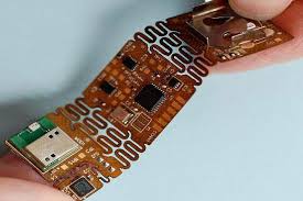
Applications Of Expose Copper Flex PCB In Wearable Technology
Expose copper flex PCBs, or flexible printed circuit boards with exposed copper traces, have become increasingly significant in the realm of wearable technology. These advanced components offer a unique combination of flexibility, durability, and electrical performance, making them ideal for a variety of applications in this rapidly evolving field. As wearable devices continue to shrink in size while expanding in functionality, the role of expose copper flex PCBs becomes ever more critical.
One of the primary applications of expose copper flex PCBs in wearable technology
is in fitness trackers. These devices, which monitor physical activity, heart rate, and other health metrics, require a high degree of flexibility to conform to the contours of the human body. Expose copper flex PCBs provide the necessary pliability without compromising on electrical performance. The exposed copper traces facilitate efficient signal transmission, ensuring that the data collected by sensors is accurately relayed to the device’s processing unit. This capability is essential for delivering real-time feedback to users, thereby enhancing the overall user experience.
In addition to fitness trackers, expose copper flex PCBs are also integral to the development of smartwatches.
These multifunctional devices combine the features of traditional timepieces with advanced computing capabilities, such as notifications, GPS tracking, and even mobile payments. The compact design of smartwatches necessitates the use of components that can be bent and folded without breaking. Expose copper flex PCBs meet this requirement, allowing for the integration of complex circuitry within a limited space. Moreover, the exposed copper traces contribute to improved thermal management, which is crucial for maintaining the device’s performance and longevity.
Another noteworthy application of expose copper flex PCBs is in medical wearables.
These devices, which include continuous glucose monitors and wearable ECG monitors, play a vital role in patient care by providing continuous health monitoring. The flexibility of expose copper flex PCBs enables these medical wearables to be comfortably worn for extended periods, thereby ensuring consistent data collection. Furthermore, the exposed copper traces enhance the reliability of signal transmission, which is paramount for accurate health monitoring. This reliability is particularly important in medical applications, where even minor inaccuracies can have significant consequences.
The use of expose copper flex PCBs extends beyond consumer and medical wearables to include applications in augmented reality (AR) and virtual reality (VR) headsets.
These devices, which are gaining popularity in both entertainment and professional settings, require lightweight and flexible components to ensure user comfort. Expose copper flex PCBs provide the necessary flexibility and durability, allowing for the seamless integration of sensors, displays, and other electronic components. The exposed copper traces also facilitate high-speed data transmission, which is essential for delivering immersive AR and VR experiences.
In conclusion, expose copper flex PCBs are indispensable in the development of wearable technology. Their unique combination of flexibility, durability, and electrical performance makes them ideal for a wide range of applications, from fitness trackers and smartwatches to medical wearables and AR/VR headsets. As wearable technology continues to advance, the demand for expose copper flex PCBs is expected to grow, further underscoring their importance in this dynamic field. By enabling the creation of smaller, more powerful, and more reliable wearable devices, expose copper flex PCBs are helping to shape the future of technology.
Design Considerations For Expose Copper Flex PCB
When designing an exposed copper flex PCB, several critical considerations must be taken into account to ensure optimal performance and reliability. The unique properties of flexible printed circuit boards (PCBs) offer numerous advantages, such as reduced weight, space savings, and enhanced flexibility, making them ideal for a wide range of applications. However, these benefits come with specific design challenges that must be addressed to fully leverage the potential of exposed copper flex PCBs.
To begin with, material selection is paramount.
The choice of substrate material significantly impacts the flexibility, durability, and thermal performance of the PCB. Polyimide is a commonly used substrate due to its excellent thermal stability, mechanical strength, and flexibility. It is crucial to select a substrate that can withstand the environmental conditions the PCB will be exposed to, including temperature variations, humidity, and mechanical stress. Additionally, the adhesive used to bond the copper to the substrate must be carefully chosen to ensure strong adhesion and reliability over the product’s lifespan.
Another important consideration is the thickness of the copper layer.
The copper thickness affects the current-carrying capacity, flexibility, and overall performance of the PCB. Thicker copper layers can handle higher currents but may reduce flexibility, while thinner layers enhance flexibility but may not support high current loads. Therefore, a balance must be struck based on the specific requirements of the application. It is also essential to consider the potential for copper oxidation, which can degrade the performance of the PCB over time. Protective coatings or surface treatments, such as immersion tin or gold plating, can be applied to exposed copper areas to mitigate oxidation and enhance durability.
The layout and routing of traces on an exposed copper flex PCB require meticulous planning.
Trace width and spacing must be optimized to ensure signal integrity and minimize electromagnetic interference (EMI). Sharp bends and tight corners should be avoided, as they can introduce stress points that may lead to mechanical failure. Instead, smooth curves and gradual transitions are recommended to maintain the integrity of the copper traces. Additionally, the use of ground planes and shielding can help reduce EMI and improve overall performance.
Thermal management is another critical aspect of designing exposed copper flex PCBs.
The flexible nature of these PCBs can make heat dissipation more challenging compared to rigid PCBs. Effective thermal management strategies, such as the use of thermal vias, heat sinks, and proper ventilation, must be incorporated into the design to prevent overheating and ensure reliable operation. The thermal conductivity of the substrate material and the copper layer also play a significant role in managing heat dissipation.
Mechanical considerations are equally important in the design of exposed copper flex PCBs.
The PCB must be able to withstand repeated flexing and bending without compromising its performance. This requires careful attention to the bend radius, which is the minimum radius the PCB can be bent without causing damage. The bend radius should be as large as possible to minimize stress on the copper traces and substrate. Additionally, the use of stiffeners or reinforcement materials in critical areas can help enhance mechanical stability and prevent damage during installation and operation.
In conclusion, designing an exposed copper flex PCB involves a comprehensive understanding of material properties, electrical and thermal performance, and mechanical durability. By carefully considering these factors and implementing best practices in layout, routing, and thermal management, designers can create reliable and high-performance flex PCBs that meet the demands of various applications. The unique advantages of exposed copper flex PCBs make them a valuable solution in the ever-evolving landscape of electronic design.