Fabrication of PCB Using the Heat Transfer Method
Abstract
Printed Circuit Boards (PCBs) are essential components in modern electronics, providing a platform for mounting and interconnecting electronic components. While various methods exist for PCB fabrication, the heat transfer method (also known as the toner transfer method) is a popular, low-cost, and accessible technique for hobbyists and small-scale production. This paper explores the step-by-step process of PCB fabrication using the heat transfer method, discussing materials, tools, advantages, limitations, and potential improvements.
1. Introduction
PCBs serve as the backbone of electronic circuits, allowing for compact and reliable connections between components. Traditional PCB manufacturing involves chemical etching, photolithography, or milling, which may require expensive equipment or hazardous chemicals. In contrast, the heat transfer method offers a simpler and more economical approach, particularly suitable for prototyping and DIY projects.
The heat transfer method involves printing a PCB layout onto a special paper (or glossy magazine paper) using a laser printer, then transferring the toner onto a copper-clad board using heat and pressure. The board is then etched to remove excess copper, leaving behind the desired circuit traces.
2. Materials and Tools Required
To fabricate a PCB using the heat transfer method, the following materials and tools are necessary:
- Copper-clad laminate – The base material for the PCB, typically FR-4.
- Laser printer – Used to print the PCB layout on transfer paper.
- Glossy paper or specialty transfer paper – Holds the toner before transfer.
- Clothing iron or laminator – Provides heat and pressure for toner transfer.
- Ferric chloride (FeCl₃) or ammonium persulfate – Etching solution to remove unwanted copper.
- Acetone or alcohol – For cleaning the board before and after transfer.
- Fine-grit sandpaper or steel wool – For surface preparation.
- PCB design software – Such as KiCad, Eagle, or Altium Designer for designing the circuit.
- Scissors or cutter – For trimming the board.
- Plastic or glass container – For the etching process.
3. Step-by-Step Process
3.1. PCB Design
The first step is designing the circuit using PCB design software. Key considerations include:
- Trace width – Ensuring sufficient width for current handling.
- Component placement – Optimizing space and minimizing interference.
- Drill holes – Marking positions for through-hole components.
Once the design is finalized, the layout is printed in mirror image on glossy paper using a laser printer.
3.2. Preparing the Copper Board
The copper-clad board must be cleaned to ensure proper toner adhesion:
- Lightly sand the surface with fine-grit sandpaper or steel wool.
- Clean with acetone or alcohol to remove grease and oxidation.
3.3. Toner Transfer Process
- Place the printed design (toner side down) onto the copper board.
- Apply heat using a clothing iron (set to medium-high heat) or a laminator.
- If using an iron, apply firm, even pressure for 3-5 minutes, moving in circular motions.
- If using a laminator, pass the board through multiple times (5-10 passes).
- Allow the board to cool, then soak it in warm water to dissolve the paper.
- Gently rub off the paper, leaving only the toner adhered to the copper.
3.4. Etching the PCB
- Prepare the etching solution (ferric chloride is commonly used).
- Submerge the board in the solution and agitate gently to speed up the process.
- Monitor until all unwanted copper is dissolved (typically 10-30 minutes).
- Rinse the board with water and remove the toner using acetone or fine sandpaper.
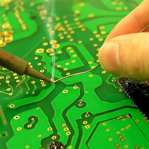
3.5. Drilling and Finishing
- Drill holes for through-hole components using a mini drill press or hand drill.
- Optionally, apply solder mask or silkscreen for professional finishing.
4. Advantages of the Heat Transfer Method
- Low cost – No need for expensive equipment.
- Quick prototyping – Suitable for DIY and educational purposes.
- No photoresist required – Simpler than UV exposure methods.
- Good resolution – Can achieve trace widths as low as 0.2 mm with proper technique.
5. Limitations and Challenges
- Inconsistent transfers – Poor heat application may lead to incomplete traces.
- Limited to single-layer PCBs – Difficult for multilayer designs.
- Environmental concerns – Etching chemicals require proper disposal.
- Lower durability – Compared to professionally manufactured PCBs.
6. Improvements and Alternatives
- Using a laminator – Provides more consistent heat and pressure than an iron.
- Higher-quality transfer paper – Improves toner adhesion.
- Alternative etching methods – Such as citric acid + hydrogen peroxide (safer than FeCl₃).
- Direct inkjet methods – Using conductive inks for simpler circuits.
7. Conclusion
The heat transfer method is an effective and economical way to produce PCBs for prototyping and small-scale projects. While it has limitations in precision and scalability, its simplicity and low cost make it a valuable technique for hobbyists and students. With proper technique and improvements, high-quality PCBs can be fabricated without expensive machinery.
For more complex or commercial applications, professional PCB manufacturing services remain the best option. However, for rapid prototyping and experimentation, the heat transfer method continues to be a practical choice.