Factors Affecting DK and Phase Consistency in PCB Circuit Boards
Abstract
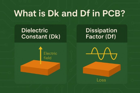
The dielectric constant (Dk) and phase consistency of printed circuit boards (PCBs) are critical parameters that influence signal integrity, especially in high-frequency and high-speed applications. Variations in Dk and phase can lead to signal distortion, impedance mismatches, and timing errors. This paper explores the key factors affecting Dk and phase consistency in PCB manufacturing, including material properties, fabrication processes, environmental conditions, and design considerations. By understanding these factors, engineers can optimize PCB performance for applications such as 5G communications, aerospace, and high-speed computing.
1. Introduction
As electronic devices operate at increasingly higher frequencies, the demand for precise control over PCB dielectric properties grows. The dielectric constant (Dk) determines the signal propagation speed, while phase consistency ensures synchronized signal transmission across different traces. Variations in these parameters can degrade signal quality, leading to increased bit error rates (BER) and reduced system reliability. This paper examines the primary factors influencing Dk and phase consistency in PCBs.
2. Material Properties
2.1 Substrate Dielectric Materials
The choice of substrate material significantly impacts Dk and phase stability. Common PCB materials include:
- FR-4: A cost-effective option but exhibits higher Dk variability with frequency.
- Rogers, PTFE, and Ceramic-filled Laminates: Offer stable Dk values but at a higher cost.
- Low-Dk Materials: Used in high-frequency applications to minimize signal delay.
Key Considerations:
- Resin Content and Reinforcement: The ratio of resin to glass fiber affects Dk uniformity.
- Filler Materials: Ceramic or silica fillers can stabilize Dk but may introduce anisotropy.
2.2 Copper Foil Roughness
The surface roughness of copper traces influences signal loss and phase response. Smoother copper reduces conductor loss but may increase manufacturing costs.
2.3 Moisture Absorption
Some substrates (e.g., polyimide) absorb moisture, increasing Dk and causing phase drift. Hydrophobic materials (e.g., PTFE) are preferred for humid environments.
3. Fabrication Process Variations
3.1 Lamination Process
Inconsistent lamination pressure and temperature can lead to variations in dielectric thickness and Dk.
3.2 Etching and Trace Geometry
- Impedance Control: Variations in trace width and spacing affect signal propagation.
- Etch Factor: Over-etching or under-etching alters trace geometry, impacting phase consistency.
3.3 Drilling and Via Formation
- Via Stub Effects: Unused via portions can cause reflections and phase shifts.
- Plating Uniformity: Poor via plating increases insertion loss and phase distortion.
4. Environmental Factors
4.1 Temperature Effects
- Thermal Coefficient of Dk (TCDk): Some materials exhibit Dk drift with temperature changes.
- Thermal Expansion: Mismatched CTE between layers can induce mechanical stress, altering phase response.
4.2 Humidity and Oxidation
- Moisture Ingression: Increases dielectric loss and Dk.
- Copper Oxidation: Degrades signal integrity, especially at high frequencies.
5. Design Considerations
5.1 Symmetrical Stackup Design
A balanced stackup minimizes warpage and ensures uniform Dk distribution.
5.2 Differential Pair Routing
- Length Matching: Critical for maintaining phase alignment in high-speed signals.
- Crosstalk Mitigation: Reduces unwanted coupling that can distort phase.
5.3 Grounding and Shielding
Proper grounding reduces electromagnetic interference (EMI), which can affect phase consistency.
6. Measurement and Testing Challenges
6.1 Test Methods for Dk and Phase
- Resonance Methods: Provide accurate Dk measurements but require precise sample preparation.
- Time-Domain Reflectometry (TDR): Useful for evaluating impedance and phase response.
6.2 Fixture and Calibration Errors
Inconsistent test setups can introduce measurement inaccuracies.
7. Mitigation Strategies
7.1 Material Selection
- Use low-loss, stable Dk materials for high-frequency designs.
- Implement moisture-resistant coatings where necessary.
7.2 Process Control
- Tighten tolerances in etching and lamination.
- Use laser drilling for precise via formation.
7.3 Environmental Protection
- Conformal coatings can shield PCBs from humidity.
- Thermal management solutions (e.g., heatsinks) stabilize operating temperatures.
8. Conclusion
Maintaining consistent Dk and phase response in PCBs requires a holistic approach, considering material properties, fabrication processes, environmental conditions, and design optimization. As signal speeds continue to rise, advancements in substrate materials and manufacturing techniques will be essential for ensuring reliable PCB performance.


