Factors Influencing the Cost of PCB Cloning
Introduction
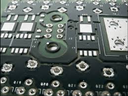
Printed Circuit Board (PCB) cloning, also known as PCB copying or PCB reverse engineering, is a process that involves recreating an existing PCB design through analysis and replication. This practice is common in electronics manufacturing for purposes such as legacy system maintenance, competitive analysis, or intellectual property investigation. The cost of PCB cloning services can vary significantly depending on multiple factors. Understanding these cost determinants helps businesses budget appropriately and make informed decisions when commissioning PCB cloning projects.
This article examines the key factors that influence PCB cloning costs, providing electronics manufacturers, engineers, and procurement specialists with comprehensive insights into the pricing structure of PCB copying services.
1. Complexity of the Original PCB Design
The complexity of the original PCB design is perhaps the most significant factor affecting cloning costs.
1.1 Layer Count
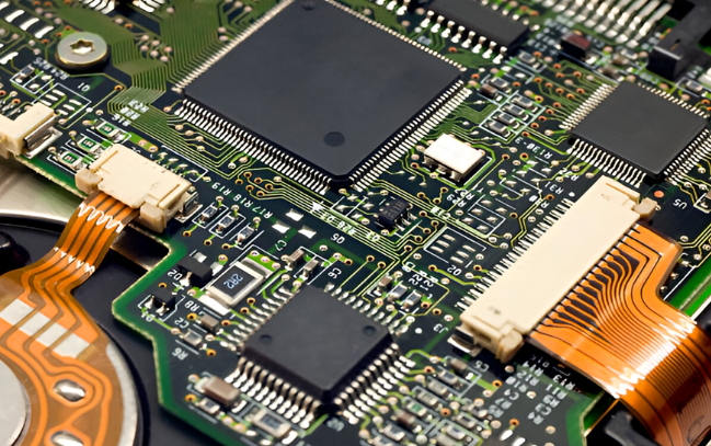
Multi-layer PCBs (typically 2-32 layers) require substantially more work to clone than simple single-sided boards. Each additional layer:
- Increases scanning and imaging time
- Requires more precise layer alignment during reconstruction
- Demands more sophisticated analysis to trace connections between layers
Cost increases are generally nonlinear—a 4-layer board may cost 2-3 times more to clone than a 2-layer board, while an 8-layer board could be 5-6 times more expensive.
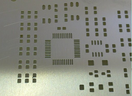
1.2 Component Density
High-density designs with:
- Miniature components (0402, 0201 packages or smaller)
- Fine-pitch ICs (under 0.5mm pitch)
- Ball Grid Array (BGA) components
- Embedded components
require higher magnification imaging, more precise measurement, and often specialized equipment, all adding to service costs.
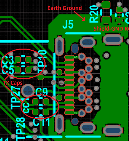
1.3 Trace Geometry
Designs featuring:
- Ultra-fine traces (under 4 mil width/space)
- Impedance-controlled traces
- High-frequency RF circuits
- Differential pairs
demand more sophisticated analysis and recreation, increasing engineering time and costs.
2. Board Physical Characteristics
2.1 Board Dimensions
Larger PCBs:
- Require more scanning time
- May need specialized scanning equipment
- Often have more components to document
- May require image stitching for high-resolution capture
2.2 Board Thickness
Thicker boards (over 2.4mm) or unusual thicknesses may require:
- Specialized delamination techniques
- Custom fixturing for scanning
- Extended processing time
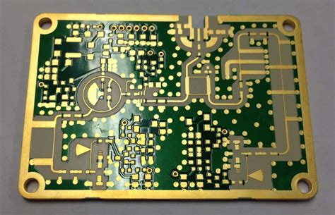
2.3 Material Type
Exotic substrate materials like:
- Rogers or other high-frequency materials
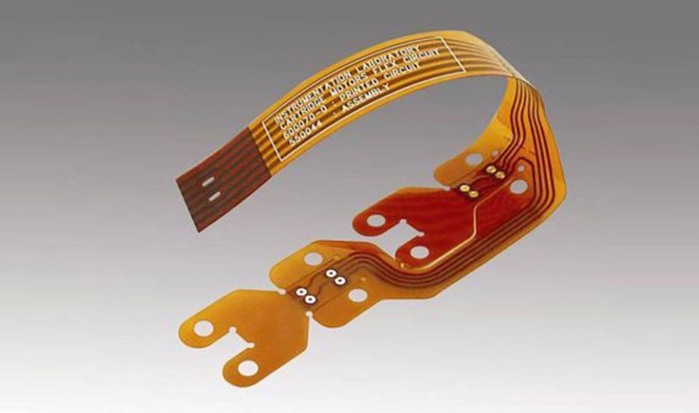
- Flexible or rigid-flex materials
- Metal-core boards
- Ceramic substrates
require specialized handling and analysis, increasing costs compared to standard FR4 boards.
3. Component Identification Requirements
3.1 Component Documentation Level
Basic cloning might only require:
- Component placement
- General part identification
While comprehensive cloning may need:
- Complete bill of materials (BOM)
- Manufacturer part numbers
- Equivalent component cross-references
- Obsolete component identification and alternatives
3.2 Component Types
Special components increase costs:
- Programmable devices (FPGAs, CPLDs, microcontrollers)
- Custom ASICs
- Obsolete or proprietary components
- Components requiring decapping or internal analysis
3.3 Marking Interpretation
Components with:
- Proprietary markings
- Obscured markings
- Removed markings
- Counterfeit markings
require additional research and analysis time to properly identify.
4. Deliverable Requirements
4.1 Output File Formats
Basic deliverables might include:
- Gerber files
- Drill files
- Simple netlist
While advanced requirements could involve:
- Full schematic recreation
- CAD files in specific formats (Altium, Eagle, KiCad, etc.)
- 3D models
- Manufacturing documentation
- Test point documentation
4.2 Documentation Depth
The extent of documentation affects costs:
- Basic placement documentation
- Complete schematic with annotations
- Functional descriptions
- Signal analysis
- Design rule documentation
4.3 Intellectual Property Considerations
Projects requiring:
- Patent circumvention analysis
- Clean room design techniques
- Legal documentation
incur additional costs for specialized expertise and procedures.
5. Technical Challenges
5.1 Board Condition
Damaged or modified boards present challenges:
- Burned or corroded areas
- Previously reworked sections
- Missing components
- Board warping or delamination
5.2 Access Restrictions
Some designs incorporate:
- Epoxy potting or conformal coatings
- Tamper-proof coatings
- Security mesh layers
- Active protection circuits
requiring specialized removal or analysis techniques.
5.3 Reverse Engineering Difficulty
Certain designs employ:
- Obfuscation techniques
- Custom component configurations
- Unusual layer stackups
- Proprietary interfaces
that complicate the reverse engineering process.
6. Service Provider Factors
6.1 Expertise and Reputation
Providers with:
- Extensive experience
- Specialized equipment
- Proven track record
- Security certifications
typically command higher prices but offer better quality and reliability.
6.2 Location
Geographical factors affect costs:
- Labor costs in provider’s region
- Shipping costs for physical boards
- Local regulations affecting the service
6.3 Turnaround Time
Expedited services often carry premium pricing:
- Standard turnaround (2-4 weeks)
- Rush service (1-2 weeks)
- Emergency service (under 1 week)
7. Additional Services
7.1 Testing and Verification
Additional services like:
- Functional testing
- Signal integrity analysis
- Thermal analysis
- Design validation
add to project costs but provide valuable verification.
7.2 Redesign Services
Many projects require:
- Design optimization
- Component substitution
- Technology updating
- Manufacturing adaptation
which go beyond basic cloning.
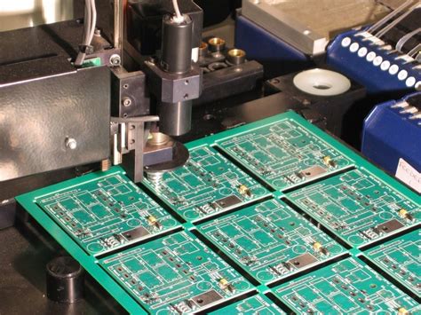
7.3 Prototyping and Manufacturing Support
Some providers offer:
- Prototype fabrication
- Small-batch production
- Full-scale manufacturing
as part of package deals.
8. Legal and Compliance Factors
8.1 Intellectual Property Considerations
Projects requiring:
- Patent analysis
- Legal opinion
- Design circumvention
involve additional legal expertise costs.
8.2 Export Controls
Certain technologies may require:
- Export license verification
- Compliance documentation
- Restricted access protocols
adding administrative costs.
Conclusion
PCB cloning costs are influenced by a complex interplay of technical, logistical, and commercial factors. The primary cost drivers include the PCB’s physical and electrical complexity, component identification requirements, deliverable specifications, and project timelines. Additional considerations such as the service provider’s capabilities, location, and value-added services further affect pricing.
Understanding these factors enables more accurate budgeting and facilitates productive discussions with service providers. For optimal results, clients should clearly communicate their requirements, expected deliverables, and any constraints at the project outset. While cost is an important consideration, the quality and completeness of the cloned design should remain paramount, particularly for critical applications.
As PCB technology continues advancing with higher densities, more sophisticated materials, and increasingly complex architectures, the art and science of PCB cloning will continue evolving—and with it, the economic factors surrounding this specialized service.