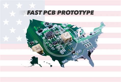
Fast PCB Prototyping: Balancing Speed and Precision

Key Takeaways
When navigating PCB manufacturing for prototyping, you’ll face critical tradeoffs between speed and precision. While 24-hour builds accelerate development cycles, they demand rigorous design validation to avoid costly revisions. Leading PCB manufacturing companies achieve 0.3mm trace precision by combining advanced laser drilling with automated optical inspection (AOI), but tighter tolerances often increase PCB manufacturing cost by 15–25%.
To optimize budgets, consider these strategies:
| Factor | Speed-Focused | Precision-Focused |
|---|---|---|
| Turnaround Time | 24–48 hours | 5–7 days |
| Minimum Trace Width | 0.4mm | 0.2mm |
| Cost per cm² | $2–$3 | $4–$6 |
“Rushing prototypes without design checks risks compounding errors. Always simulate thermal and signal integrity before finalizing layouts.” – Industry Expert
For global projects, Eastern European PCB manufacturing business hubs offer a unique balance of competitive pricing and ISO-certified quality, particularly for high-mix, low-volume orders. Whether prioritizing rapid iteration or micron-level accuracy, align your approach with end-use requirements—consumer electronics tolerate wider tolerances, while medical or aerospace prototypes demand stricter specs. By pre-validating designs and selecting partners with transparent PCB manufacturing cost structures, you mitigate risks without sacrificing timelines.
Fast PCB Prototyping: Speed vs Precision
When prioritizing PCB manufacturing timelines, you might face tradeoffs between rapid delivery and exacting specifications. While 24-hour turnaround services excel for urgent iterations, achieving 0.3mm trace precision demands advanced processes that can strain tight deadlines. Reputable PCB manufacturing companies often deploy automated optical inspection (AOI) systems to maintain accuracy without sacrificing speed, but thinner traces or complex multilayer designs may still require additional validation steps.
Balancing PCB manufacturing cost with precision becomes critical here. For instance, opting for standard FR-4 materials and larger via sizes accelerates production, whereas high-density interconnects (HDIs) or controlled impedance routing could extend lead times. To optimize outcomes, align your design parameters with your prototype’s purpose—functional testing might tolerate minor tolerances, while RF or high-speed boards demand tighter margins.
Even in fast-turn PCB manufacturing business models, communication is key. Clarify your critical tolerances upfront to avoid revisions, and leverage pre-validated design rules from your supplier. This ensures your prototype meets both deadlines and performance benchmarks, bridging the gap between speed and precision before full-scale production.
24-Hour PCB Builds: Balancing Quality
When opting for 24-hour PCB builds, you’re prioritizing speed, but maintaining quality remains non-negotiable. Leading PCB manufacturing companies achieve this balance by integrating advanced processes like automated optical inspection (AOI) and real-time impedance control. These systems catch defects early, ensuring even rapid-turn boards meet ±0.1mm layer alignment tolerances. However, accelerating production cycles requires meticulous planning—overlooking design rule checks (DRC) to save time often backfires, leading to costly revisions.
To minimize PCB manufacturing cost without sacrificing reliability, consider panelizing designs or standardizing materials. Many providers offer tiered pricing for bulk orders, but for prototypes, modular tooling allows faster setup times. This efficiency is why partnering with experienced PCB manufacturing business operators matters: they optimize workflows to prevent compromises like uneven copper plating or solder mask peeling.
Remember, speed in prototyping isn’t just about machinery—it’s about expertise. Skilled engineers review your files pre-production, flagging potential thermal or signal integrity issues. This proactive approach ensures your 24-hour build aligns with final-product requirements, avoiding delays in later stages. By aligning your priorities with a manufacturer’s technical capabilities, you secure both velocity and precision.

0.3mm Trace Precision: Technical Challenges
Achieving 0.3mm trace precision requires navigating tight tolerances that test the limits of modern PCB manufacturing processes. For PCB manufacturing companies, maintaining this level of accuracy while delivering rapid turnaround involves balancing advanced equipment with meticulous process control. Etching techniques must account for material behavior under high-speed production, as even minor deviations in copper thickness or resist application can compromise trace integrity.
The challenge intensifies when aligning multilayer boards, where registration errors as small as 0.05mm can disrupt signal paths. To mitigate this, manufacturers often deploy laser direct imaging (LDI) systems, though these technologies raise PCB manufacturing cost due to their precision-focused operation. You’ll also encounter tradeoffs in material selection—high-frequency substrates may enhance performance but demand slower processing speeds, conflicting with fast prototyping goals.
For businesses optimizing PCB manufacturing business workflows, investing in automated optical inspection (AOI) becomes critical. These systems verify trace widths and spacing in real time, reducing rework rates. However, integrating such tools without inflating project timelines requires careful calibration. By understanding these technical hurdles, you can better evaluate vendors’ capabilities and ensure your designs meet both speed and precision benchmarks.

Cost-Effective Prototyping From 2 Strategies
When optimizing PCB manufacturing costs, two strategic approaches let you maintain quality without overspending. First, design simplification reduces material waste and production complexity. By collaborating with PCB manufacturing companies early in the design phase, you can identify features that inflate costs—like unnecessary multilayer boards or ultra-fine traces—and adjust them before prototyping. For instance, using standard FR-4 substrates instead of high-frequency laminates can cut material expenses by 15–30% while still meeting functional requirements.
Second, leverage batch ordering to lower per-unit costs. Many PCB manufacturing businesses offer tiered pricing, where ordering 5–10 prototype boards instead of a single unit reduces the PCB manufacturing cost by up to 40%. This strategy works particularly well when validating designs across multiple iterations, as bulk orders amortize setup fees. However, balance this with your timeline: while faster turnarounds (like 24-hour builds) prioritize speed, they may limit bulk discounts. Transitioning to pre-production validation becomes smoother when these cost-control methods align with your project’s technical and budgetary constraints.
Pre-Production Design Validation Techniques
Before committing to full-scale PCB manufacturing, validating your design’s functionality and manufacturability is critical. Start by running electrical rule checks (ERC) and design for manufacturability (DFM) analyses to identify potential flaws in trace spacing, component placement, or thermal management. Many PCB manufacturing companies offer automated DFM feedback, highlighting issues like insufficient clearance for 0.3mm traces or impedance mismatches that could delay production.
Leverage simulation tools to model signal integrity and power distribution, especially for high-speed or high-frequency designs. Prototyping a small batch through rapid-turn services allows physical testing under real-world conditions, revealing hidden thermal stresses or EMI interference. This step helps avoid costly revisions later, directly impacting PCB manufacturing cost efficiency.
Collaborate early with your PCB manufacturing business partner to align design choices with their capabilities. For instance, specifying materials with shorter lead times or optimizing panel layouts can accelerate turnaround without sacrificing precision. By addressing these factors pre-production, you reduce the risk of respins while maintaining the balance between speed and accuracy demanded by fast-paced development cycles.
Global PCB Services: Speed & Accuracy
When sourcing PCB manufacturing services globally, you’ll find regional variations in turnaround times and technical capabilities. Leading PCB manufacturing companies in North America and Europe often prioritize precision, leveraging advanced machinery to achieve 0.3mm trace tolerances even for 24-hour builds. Meanwhile, Asian suppliers frequently optimize PCB manufacturing cost through high-volume workflows, though this can introduce tradeoffs in customization flexibility. To balance speed and accuracy, evaluate providers’ certifications (e.g., ISO 9001) and their capacity to handle complex designs without inflating timelines.
Modern PCB manufacturing business models increasingly integrate real-time tracking systems, allowing you to monitor production stages remotely—critical for maintaining quality control across borders. For time-sensitive projects, Eastern European hubs have emerged as competitive alternatives, offering 48-hour prototyping with lower logistics costs compared to transcontinental shipping. However, always verify material sourcing practices: substandard substrates can compromise signal integrity, negating the benefits of rapid delivery. By aligning your design’s complexity with a supplier’s core strengths, you mitigate risks while capitalizing on globalized efficiencies.
DIY vs Professional Prototyping Tradeoffs
When choosing between DIY and professional pcb manufacturing, you’ll face critical tradeoffs in capability, time, and quality. For simple designs with relaxed tolerances, DIY methods using basic etching kits or desktop milling machines might suffice, offering immediate control over iterations. However, as complexity increases—especially with 0.3mm trace precision or multilayer requirements—the limitations of home setups become apparent. Professional pcb manufacturing companies leverage industrial-grade equipment like laser direct imaging (LDI) and automated optical inspection (AOI), ensuring consistency that’s nearly impossible to replicate manually.
Cost comparisons reveal another layer: while DIY avoids upfront pcb manufacturing cost for small batches, it risks hidden expenses from material waste or design flaws. Professional services, though pricier per board, often include design validation and expert feedback to prevent costly revisions later. For startups or scaled operations, partnering with a pcb manufacturing business becomes strategic—outsourcing not only accelerates timelines but also frees engineering resources for core R&D. Yet, hobbyists or educators might prioritize hands-on learning over perfection, accepting minor imperfections for educational value. The key lies in aligning your approach with project goals: speed and precision demand professionals, while experimental builds tolerate DIY tradeoffs.
Eastern Europe PCB Turnaround Solutions
When exploring global options for PCB manufacturing, Eastern Europe emerges as a strategic partner for balancing rapid turnaround with technical precision. Regional PCB manufacturing companies leverage advanced automation and proximity to Western markets to deliver prototypes in as little as 48 hours, often at PCB manufacturing costs 15-20% lower than counterparts in North America or Western Europe. This efficiency stems from streamlined logistics and vertically integrated facilities that minimize delays in material sourcing.
For designs requiring 0.3mm trace precision, Eastern European manufacturers employ laser direct imaging (LDI) systems paired with rigorous quality checks, ensuring compliance with international standards. While speed is prioritized, these providers maintain flexibility for last-minute design adjustments—a critical advantage during pre-production validation. However, balancing affordability and capability requires careful vetting: smaller PCB manufacturing business operators may lack certifications for high-frequency or military-grade applications.
By aligning your project’s complexity with regional specializations, you can optimize both timelines and budgets without compromising on critical specifications. This approach complements broader strategies for cost-effective prototyping while maintaining a global supply chain resilience.
Conclusion
When navigating the final stages of PCB manufacturing, it becomes clear that balancing speed and precision requires strategic planning. Leading PCB manufacturing companies leverage advanced technologies to deliver 24-hour turnarounds without compromising on 0.3mm trace accuracy, but your design choices ultimately determine cost and quality outcomes. By validating layouts pre-production and selecting suppliers with transparent PCB manufacturing cost structures, you avoid costly revisions while maintaining tight deadlines.
For startups or smaller teams, partnering with a PCB manufacturing business specializing in rapid prototyping ensures access to industrial-grade capabilities without upfront capital investments. However, weigh this against DIY approaches if your project tolerates slightly longer lead times for lower-volume testing. Regardless of your path, prioritize vendors offering clear communication channels and real-time progress tracking—critical factors when timelines are measured in hours, not days.
Remember, the right balance hinges on aligning technical requirements with budgetary constraints. By understanding how speed-driven workflows interact with precision thresholds, you’ll streamline iterations and accelerate product launches without sacrificing reliability.
FAQs
How does fast PCB prototyping maintain precision during 24-hour builds?
Advanced PCB manufacturing workflows combine automated optical inspection (AOI) and real-time impedance control, ensuring 0.3mm trace widths meet design specs. Reputable PCB manufacturing companies prioritize multi-stage verification to balance speed with accuracy.
What drives PCB manufacturing cost for rapid prototypes?
Material selection, layer count, and surface finishes account for 70% of expenses. Low-volume PCB manufacturing business models often reduce overhead by optimizing panel utilization, with some services offering rates from $2 per square inch for 2-layer boards.
When should you choose professional prototyping over DIY methods?
While DIY kits work for simple circuits, professional PCB manufacturing ensures compliance with IPC-6012 standards for high-frequency or densely packed designs. Complex layouts requiring blind vias or controlled-depth drilling demand industrial-grade equipment.
Can global PCB manufacturing companies guarantee both speed and consistency?
The emergence of decentralized production hubs—particularly in Eastern Europe—enables 3-day deliveries to EU/US markets. Leading providers synchronize DFM checks across regions, maintaining ≤5% tolerance variance in impedance-controlled boards.
How do pre-production validations reduce prototyping risks?
Automated design-for-manufacturability (DFM) tools flag spacing violations and thermal imbalances before fabrication. Many PCB manufacturing partners offer free file reviews, preventing 85% of common errors that delay builds.
Accelerate Your Project With Reliable PCB Manufacturing
Ready to optimize your prototype’s timeline without compromising quality? Visit our PCB manufacturing portal for instant quotes and expert design support—click here to start your next build.