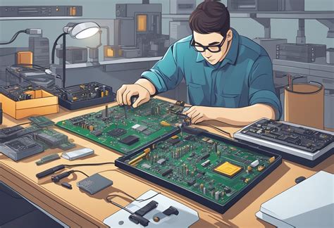
Fast Turnaround PCB Assembly: Accelerating Prototype to Produ
Key Takeaway
The strategic advantage of PCB assembly services lies in their ability to compress development timelines without compromising technical rigor. By leveraging PCBA processes with rapid prototyping capabilities, engineers can iterate designs in days rather than weeks, directly addressing flaws in initial concepts. This accelerated approach eliminates traditional bottlenecks, as shown in the comparison below:
| Traditional Workflow | Fast-Turn PCB Assembly |
|---|---|
| 4-6 week lead times | 48-hour to 5-day turnaround |
| Limited design iterations | 3-5x more prototype revisions |
| High upfront tooling costs | Flexible low-volume production |
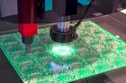
Such efficiency enables teams to validate functional requirements earlier while synchronizing with component sourcing and DFM (Design for Manufacturing) checks. For startups and established firms alike, PCBA solutions transform time-to-market from a constraint into a competitive lever—particularly critical in sectors like IoT and medical devices where regulatory approvals demand multiple validation cycles. Modern providers achieve this velocity through automated optical inspection (AOI) systems and just-in-time material management, ensuring zero compromises on solder joint integrity or signal stability. By compressing development phases that previously spanned quarters into weeks, businesses gain crucial windows to refine user experiences or respond to emerging market demands.
Fast PCB Assembly Speeds Product Development
Rapid PCB assembly services have become a cornerstone of modern electronics development, enabling teams to compress timelines without compromising quality. By leveraging advanced PCBA workflows, engineers can transform prototypes into market-ready products in days rather than weeks. This acceleration is particularly critical in industries like IoT, wearables, and medical devices, where time-to-market directly impacts competitive advantage.
Tip: Integrate design-for-manufacturing (DFM) checks early in the prototyping phase to avoid revisions during PCB assembly, preserving both speed and budget.
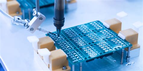
The synergy between automated pick-and-place systems and precision soldering technologies ensures that even complex multilayer boards undergo PCBA with <200ppm defect rates. Real-time component tracking systems further eliminate procurement delays, a common bottleneck in traditional assembly pipelines. For startups, this agility translates to faster investor demonstrations, while established firms benefit from accelerated iteration cycles for feature enhancements.
Transitioning smoothly from prototyping to mass production requires alignment between PCB assembly partners and product teams. Advanced providers now offer concurrent engineering support, resolving potential manufacturability issues before the first board is populated. This proactive approach reduces the validation-to-production gap by up to 40%, according to recent industry benchmarks.

Rapid Prototyping Through Quick-Turn PCB Solutions
The ability to rapidly transform design concepts into functional prototypes is critical in modern electronics development. PCB assembly services specializing in quick-turn solutions enable engineers to iterate designs efficiently, reducing traditional lead times from weeks to days. By leveraging advanced PCBA workflows—including automated component placement and precision soldering—teams can validate circuit performance, thermal management, and form factor compatibility early in the design cycle.
Iterative design benefits significantly from accelerated prototyping, as engineers identify and resolve issues like signal interference or power distribution flaws before final production. For startups and R&D departments, this agility translates to faster validation of innovative features, whether for IoT devices or high-frequency communication systems. Modern quick-turn PCB assembly providers combine speed with rigorous testing protocols, ensuring prototypes meet functional specifications despite compressed timelines.
A key advantage lies in the seamless transition from prototype to scaled manufacturing. Suppliers offering dual-track services can refine PCBA processes during prototyping, preemptively addressing potential bottlenecks in mass production. This synergy between rapid prototyping and manufacturing readiness is particularly valuable in industries like automotive electronics and medical devices, where regulatory compliance and reliability are non-negotiable.
By compressing the feedback loop between design and testing, quick-turn PCB solutions empower teams to explore multiple design permutations without sacrificing project schedules—a decisive factor in maintaining competitive momentum.
Cutting Time-to-Market With Accelerated PCB Assembly
In today’s hypercompetitive electronics landscape, PCB assembly speed directly impacts a product’s commercial viability. By leveraging accelerated PCBA workflows, manufacturers compress development cycles from weeks to days, enabling rapid iterations that align with evolving market demands. Advanced automated pick-and-place systems and just-in-time component sourcing eliminate bottlenecks, ensuring seamless transitions from design validation to full-scale production. For startups and enterprises alike, this agility translates to first-mover advantages—critical in industries like IoT and wearable tech where timing defines success.
Strategic partnerships with PCB assembly providers specializing in quick-turn solutions further enhance efficiency. These collaborators employ real-time DFM (Design for Manufacturing) feedback, preempting redesign delays while maintaining rigorous quality standards. Additionally, modular prototyping allows parallel testing of subsystems, slashing validation phases by up to 40%. Crucially, accelerated timelines don’t compromise reliability; automated optical inspection (AOI) and in-line testing protocols ensure defect rates remain below 0.1%, even under tight deadlines. By integrating speed with precision, businesses transform PCBA from a production step into a strategic accelerator, securing market share before competitors finalize their first prototypes.
How Fast-Turn PCB Services Boost Innovation Cycles
The relentless pace of technological advancement demands agile development strategies, where PCB assembly speed becomes a critical enabler of innovation. By compressing iteration timelines, fast-turn PCBA services allow engineers to test multiple design variations within days rather than weeks. This acceleration directly impacts R&D efficiency—teams can identify functional flaws earlier, refine power distribution networks faster, and validate signal integrity improvements in near-real time.
For startups racing against funding cycles or enterprises managing parallel product lines, rapid PCB assembly transforms prototyping from a bottleneck into a strategic asset. Consider emerging IoT devices: a 5-day PCB assembly turnaround enables three complete design iterations within a typical two-week sprint, dramatically increasing first-pass success rates. This velocity extends to component validation phases, where quick-turn services support A/B testing of alternative ICs or connector configurations without derailing project schedules.
Moreover, the synergy between fast PCBA and automated testing frameworks creates closed-loop innovation systems. Manufacturers utilizing machine vision inspection and in-line functional testing can feed performance data back to design teams within 48 hours, creating tighter feedback loops. This approach is particularly transformative in sectors like medical wearables, where regulatory compliance requires exhaustive validation—every saved day in PCB assembly translates to earlier clinical trials and faster certification processes.
By eliminating traditional manufacturing delays, quick-turn PCB services effectively redistribute time resources toward creative problem-solving, allowing engineering teams to focus on performance optimization rather than logistical coordination. This paradigm shift is redefining competitiveness across industries, turning PCB iteration speed into a measurable innovation metric.
Optimizing PCB Assembly for Faster Product Launches
Achieving accelerated product launches hinges on streamlining PCB assembly workflows without compromising precision. By integrating design for manufacturing (DFM) principles early in the prototyping phase, engineers can preemptively address potential bottlenecks in PCBA processes. Advanced manufacturers leverage automated optical inspection (AOI) systems and real-time production monitoring to minimize rework cycles, ensuring that high-volume transitions maintain the same rigor as prototype builds.
A critical factor lies in material sourcing strategies. Partnering with suppliers that guarantee rapid component availability reduces delays caused by obsolete or long-lead-time parts. Simultaneously, adopting modular PCB assembly designs allows for parallel testing of subsystems, compressing validation timelines. For instance, signal integrity checks and thermal performance assessments can occur concurrently with final assembly stages.
Moreover, optimizing panelization layouts to maximize board yield per panel not only cuts material waste but also accelerates batch processing. This approach, combined with just-in-time inventory practices, ensures that PCBA timelines align seamlessly with broader production schedules. By balancing these technical and logistical refinements, companies can shave weeks off development cycles, transforming agile prototyping into market-ready solutions at unprecedented speeds.
Streamlining Prototyping With Quick-Turn PCB Solutions
Modern electronics development thrives on iterative refinement, making PCB assembly speed a critical factor in prototyping efficiency. Quick-turn solutions compress traditional lead times from weeks to days, enabling engineers to validate designs and identify flaws early in the development cycle. By leveraging advanced PCBA workflows—such as automated component placement and in-line optical inspection—teams can rapidly test multiple design iterations without compromising precision.
A key advantage lies in the seamless integration of design-for-manufacturability (DFM) checks into the prototyping phase. These preemptive validations minimize rework by flagging potential issues like trace spacing errors or thermal mismatches before fabrication begins. Coupled with just-in-time material sourcing, PCB assembly partners ensure critical components are staged for immediate integration, eliminating bottlenecks caused by supply chain delays.
For startups and R&D teams, agile prototyping translates to faster feedback loops. A 5-day PCBA turnaround, for instance, allows developers to progress from schematic revisions to functional testing within a single workweek. This velocity is further amplified by hybrid manufacturing models that combine rapid prototyping tools (e.g., laser-direct imaging) with scalable production-grade processes, ensuring design continuity from prototype to mass production.
By synchronizing engineering timelines with accelerated assembly capabilities, businesses can transform theoretical concepts into market-ready innovations at unprecedented speeds—a competitive edge in industries where being first-to-market often dictates commercial success.
Fast-Turn PCB Manufacturing for Competitive Electronics
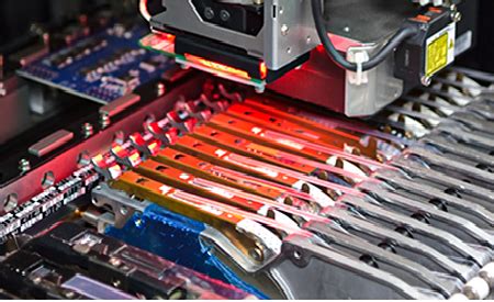
In today’s hyper-competitive electronics landscape, PCB assembly services with rapid turnaround times have become a strategic differentiator. Companies leveraging fast-turn PCBA solutions gain critical advantages by compressing production cycles, enabling them to refine prototypes and launch products weeks ahead of traditional timelines. Modern PCB assembly providers employ automated optical inspection (AOI) and advanced surface-mount technology (SMT) to maintain precision while operating at accelerated speeds—ensuring design integrity isn’t sacrificed for velocity.
For industries like IoT, wearables, and automotive electronics, where time-to-market directly impacts market share, PCBA partners offering 24-72 hour turnaround windows allow firms to iterate designs rapidly in response to real-world testing feedback. This agility is further enhanced by integrated supply chain networks that streamline material sourcing, mitigating delays from component shortages. By aligning PCB assembly speed with rigorous quality protocols, manufacturers achieve the dual objectives of accelerated production and reliability—key drivers for maintaining competitiveness in sectors governed by rapid technological obsolescence.
Balancing Speed and Quality in PCB Assembly Pr
Achieving optimal results in PCB assembly requires navigating the delicate equilibrium between accelerated production timelines and uncompromised quality. While rapid prototyping and time-to-market pressures dominate modern electronics development, cutting corners in manufacturing processes can lead to costly redesigns or field failures. Advanced PCBA providers address this challenge by integrating precision-driven workflows with agile methodologies. Automated optical inspection (AOI) systems, for instance, enable real-time defect detection without slowing down high-speed pick-and-place operations, ensuring both speed and accuracy in component placement.
Material selection plays a pivotal role in this balance—using certified substrates and lead-free solders maintains reliability standards even under compressed schedules. Seasoned manufacturers often employ design-for-manufacturability (DFM) checks early in the process to eliminate rework bottlenecks later. By combining parallel processing for multilayer boards with rigorous electrical testing protocols, PCB assembly teams can compress cycle times while adhering to IPC-A-610 Class 2/3 specifications. This approach ensures that accelerated PCBA services deliver not just speed, but production-ready prototypes that withstand thermal stress and signal integrity tests—critical for maintaining brand reputation in competitive markets.
Conclusion
In the evolving landscape of electronics manufacturing, PCB assembly services with rapid turnaround capabilities have become indispensable for innovators aiming to bridge the gap between prototyping and mass production. By leveraging advanced manufacturing techniques and streamlined supply chains, PCBA providers empower companies to compress development timelines while maintaining rigorous quality standards. This acceleration not only reduces time-to-market but also creates opportunities for iterative design improvements, ensuring products meet evolving market demands.
The strategic adoption of fast-turn PCB assembly aligns with modern industry needs, where agility often dictates competitive advantage. However, success hinges on selecting partners capable of balancing speed with precision—prioritizing factors like automated optical inspection (AOI) and functional testing even under tight deadlines. As technologies like IoT and AI drive demand for smarter electronics, the ability to rapidly transition from concept to PCBA-ready designs will remain a cornerstone of innovation. Ultimately, integrating these accelerated workflows into product development strategies enables businesses to respond dynamically to opportunities, securing their position at the forefront of technological advancement.
FAQ
How does fast-turn PCB assembly benefit prototyping phases?
Accelerated PCBA processes enable engineers to test multiple design iterations within days, identifying potential flaws early. This compression of feedback loops allows teams to refine functional specifications before final production tooling.
What quality controls exist in rapid PCB assembly services?
Reputable providers combine automated optical inspection (AOI) with X-ray verification even in expedited timelines. Many implement ISO 9001-certified workflows, ensuring signal integrity and thermal performance meet specifications despite compressed schedules.
Can complex designs maintain reliability with quick-turn PCBA?
Advanced manufacturers utilize high-density interconnect (HDI) techniques and impedance-controlled routing to handle 16+ layer boards in accelerated timelines. Component sourcing networks with real-time inventory tracking prevent delays for specialized ICs or connectors.
Accelerate Your Innovation Timeline Today
Ready to transform your product development cycle? PCB assembly experts await your project specifications. Please click here to explore tailored fast-turn solutions matching your timeline and technical requirements.