Five Methods for Reliability Design of Printed Circuit Boards
First, ground design In electronic equipment, grounding is an important method to control interference
If you can use the correct combination of grounding and shielding, you can solve most of the interference problems. The ground structure of the electronic device is roughly systematic, chassis ground (shielded ground), digital ground (logical ground), and analog ground. The following points should be noted in the grounding design:
1. The correct choice of single-point grounding and multi-point grounding In low-frequency circuits,
the operating frequency of the signal is less than 1MHz, its influence on the inductance between the wiring and the device is small, and the circulation current formed by the grounding circuit has a greater impact on the interference, and should be used Grounded at one point. When the operating frequency of the signal is greater than 10 MHz, the impedance of the ground wire becomes very large. At this time, the resistance of the ground wire should be reduced as much as possible, and the multi-point grounding should be used nearby. When the operating frequency is from 1 to 10 MHz, if a point is grounded, the length of the ground wire should not exceed 1/20 of the wavelength. Otherwise, the multi-point grounding method should be adopted.
2. Separate the digital circuit from the analog circuit.
There are both high-speed logic circuits and linear circuits on the circuit board. They should be separated as much as possible, and the ground lines of the two should not be mixed. They are connected to the power supply ground. Try to increase the grounding area of the linear circuit.
3. Try to make the grounding wire as thick as possible.
If the grounding wire is very thin, the grounding potential changes with the change of the current, causing the timing signal level of the electronic equipment to be unstable and the anti-noise performance to deteriorate. Therefore, the ground wire should be as thick as possible so that it can pass three allowable currents on the printed circuit board. If possible, the width of the grounding wire should be greater than 3mm.
4. When the grounding wire is a closed-loop design, the printed circuit board grounding system consists of only digital circuits.
Turning the grounding wire into a closed loop can significantly improve noise immunity. ability. The reason for this is that there are many integrated circuit components on the printed circuit board, especially when there are many components that consume too much power, due to the limitation of the thickness of the grounding wire, a large potential difference will be generated in the ground junction, and the anti-noise ability will decrease. If the grounding structure is looped, the potential difference will be reduced and the anti-noise capability of the electronic equipment will be improved.
Second, electromagnetic compatibility design
Electromagnetic compatibility refers to the ability of electronic devices to work in coordination and effectively in various electromagnetic environments. The purpose of the electromagnetic compatibility design is to enable electronic devices to both suppress various external interferences and enable the electronic devices to work properly in a specific electromagnetic environment while reducing the electromagnetic interference of the electronic devices themselves to other electronic devices.
1. Choose a reasonable wire width.
Because the impact interference produced by the transient current on the printed lines is mainly caused by the inductance components of the printed conductors, the inductance of the printed conductors should be minimized. The inductance of a printed conductor is proportional to its length and inversely proportional to its width, so a short, fine conductor is good for suppressing interference. Clock lines, row drivers, or bus driver signal lines often carry large transient currents. Printed conductors must be as short as possible. For a discrete component circuit, when the width of the printed conductor is about 1.5mm, it can fully meet the requirements; for the integrated circuit, the width of the printed conductor can be selected between 0.2~1.0mm.
2. Use the correct cabling strategy.
Equivalent traces can reduce the inductance of the wire, but the mutual inductance and distributed capacitance between the wires increase. If the layout allows, it is better to adopt the grid structure of the grid structure. The specific approach is to laterally route one side of the printed circuit board, and the other is to make vertical wiring. Then connect them with metallized holes at the cross holes.
In order to suppress the crosstalk between printed circuit board wires, it is necessary to avoid long-distance equal alignment in designing the wiring, and to pull the distance between the wires as much as possible. The signal wires should not intersect with the ground wire and the power supply wire as much as possible. Placing a grounded trace between signal lines that are sensitive to interference can effectively suppress crosstalk.
In order to avoid the electromagnetic radiation generated when high-frequency signals pass through the printed conductors, the following points should also be noted when wiring the printed circuit board:
● Minimize the discontinuity of printed conductors. For example, do not change the width of the conductors. The corners of the conductors should be greater than 90 degrees to prevent looping.
● The clock signal leads are most likely to cause electromagnetic radiation interference. When the cable is routed, it should be close to the ground loop. The driver should be next to the connector.
● The bus driver should be close to the bus it wants to drive. For those leads that leave the printed circuit board, the driver should hold the connector tightly.
● The data bus should be routed with a signal ground between every two signal lines. It is best to place the ground loop next to the least important address lead because the latter often carries high-frequency currents.
● When the printed circuit board is equipped with high-speed, medium-speed, and low-speed logic circuits, the devices should be arranged.
3. Suppress reflection interference.
In order to suppress the reflection interference appearing at the end of the printed line, in addition to the special needs, the length of the printed line should be shortened as much as possible and the slow circuit should be used. If necessary, terminal matching may be added, that is, a matching resistor with the same resistance is added to the ground and the power supply terminal at the end of the transmission line. According to experience, terminal matching measures should be adopted when the printed lines are longer than 10cm for TTL circuits with fast speeds. The resistance of the matching resistor should be determined based on the maximum value of the output drive current and the sink current of the integrated circuit.
Third, decoupling capacitor configuration
In a DC power circuit, changes in the load can cause power supply noise. For example, in a digital circuit, when the circuit is switched from one state to another, a large spike current is generated on the power line, forming a transient noise voltage. Configuring decoupling capacitors can suppress the noise caused by load changes. It is a common practice for the reliability design of printed circuit boards. The configuration principles are as follows:
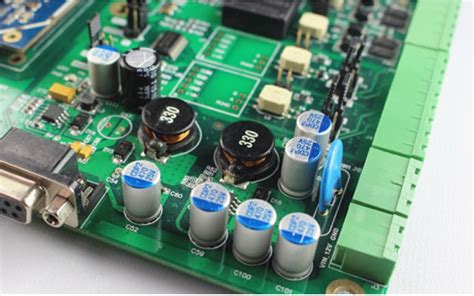
● Connect a 10-100uF electrolytic capacitor across the input of the power supply.
If the position of the printed circuit board is allowed, the anti-interference effect of the electrolytic capacitor with 100uF or more will be better.
• Configure a 0.01uF ceramic capacitor for each integrated circuit chip.
If the printed circuit board space is small and can not be installed, a 1~10uF tantalum electrolytic capacitor can be configured for every 4 to 10 chips. The high frequency impedance of this device is particularly small, and the impedance is less than 1Ω in the range of 500kHz to 20MHz. And the leakage current is very small (less than 0.5uA).
● For devices with low noise power, large current changes during turn-off, and memory devices such as ROM and RAM, decoupling capacitors should be directly connected between the power supply line (Vcc) and the ground (GND) of the chip.
● The lead of the decoupling capacitor cannot be too long, especially the high frequency bypass capacitor cannot lead
Fourth, the size of the printed circuit board and the device layout
The printed circuit board should be of a moderate size. When the printed circuit board is too large, the printed lines are long and the impedance increases. This not only reduces the ability to resist noise, but also has a high cost. When the printed circuit board is too small, the heat dissipation is not good, and it is easily disturbed by adjacent lines.
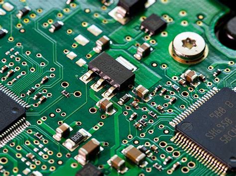
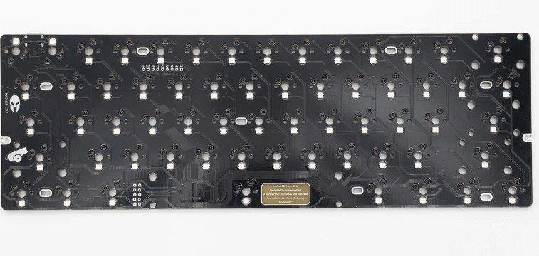
In the device layout, as with other logic circuits, the related devices should be placed as close as possible, so that a good anti-noise effect can be obtained. as shown in picture
2. The clock generators, crystal oscillators, and the CPU’s clock inputs are all prone to noise and should be close to each other.
Devices that are prone to noise, low-current circuits, high-current circuits, etc. should be as far away as possible from logic circuits. If possible, it is important to make another circuit board. This is very important.
Fifth, thermal design from the perspective of conducive to heat dissipation
The printed board is preferably mounted upright, and the distance between the board and the board should not be less than 2cm in general, and the arrangement of the device on the printed board should follow certain rules: For equipment that uses free convection air cooling, it is best to The integrated circuits (or other devices) are arranged in a lengthwise manner.
For devices employing forced air cooling, it is preferable to arrange the integrated circuits (or other devices) in a horizontally long manner. Devices on the same printed board should be arranged as much as possible according to the amount of heat generated and the degree of heat dissipation.
Devices with small heat or poor heat resistance (such as small-signal transistors, small-scale integrated circuits, electrolytic capacitors, etc.) should be placed in the cooling airflow. The most upstream (entrance), heat or good heat resistance devices (such as power transistors, large scale integrated circuits, etc.)
placed in the most downstream of the cooling airflow. In the horizontal direction, high-power devices are placed as close as possible to the edge of the printed board to shorten the heat transfer path; in the vertical direction, high-power devices are placed as close to the printed board as possible, so as to reduce the influence of the temperature of other devices when these devices work. .
Devices that are sensitive to temperature are best placed in the area with the lowest temperature (such as the bottom of the device).
Do not place it directly on the heat-generating device. Multiple devices are preferably staggered on a horizontal plane. The heat dissipation of printed boards in equipment is mainly dependent on air flow. Therefore, air flow paths should be studied during design, and devices or printed circuit boards should be properly configured.
When air flows, it tends to flow where the resistance is low. Therefore, when configuring the device on the printed circuit board, avoid leaving a large airspace in a certain area. The configuration of multiple printed circuit boards in the whole machine should also pay attention to the same problem.
A great deal of practical experience shows that using a reasonable arrangement of devices can effectively reduce the temperature rise of the printed circuit, thus significantly reducing the failure rate of devices and equipment. The above are just some of the general principles of reliability design of printed circuit boards. The reliability of the circuit board is closely related to the specific circuit. In the design, it is not necessary to perform corresponding processing according to the specific circuit in order to ensure the reliability of the printed circuit board to the greatest degree.