Flawless PCB Assembly: Critical Steps for Optimal Performance

Key Takeaways
Successful PCB assembly hinges on meticulous attention to detail across design, manufacturing, and validation stages. Component placement must prioritize signal integrity and thermal management, ensuring high-density layouts avoid interference. PCBA reliability begins with precision soldering—whether using reflow or wave techniques—to prevent cold joints or bridging.
Tip: Always validate solder paste stencil alignment before reflow to minimize rework and ensure consistent connections.
Advanced testing protocols, such as automated optical inspection (AOI) and in-circuit testing (ICT), are critical for identifying latent defects in PCB assembly. Rigorous quality control steps, including functional testing under simulated operating conditions, verify durability and performance. For optimal results, integrate design-for-manufacturing (DFM) principles early to reduce errors and streamline production.
Transitioning between these stages requires seamless coordination between design and assembly teams. By balancing technical precision with proactive problem-solving, manufacturers can achieve flawless PCBA outcomes that meet both functional and longevity benchmarks.
PCB Component Placement Essentials
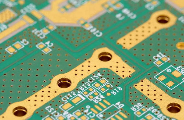
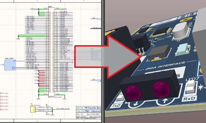
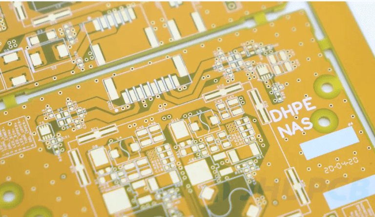
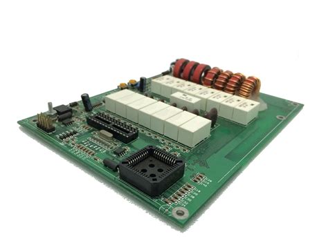
Strategic PCB component placement forms the foundation of successful PCB assembly, directly influencing performance, thermal management, and manufacturability. Properly positioning components during the PCBA process minimizes signal interference, optimizes heat dissipation, and ensures mechanical stability. Start by grouping related components (e.g., power supplies, analog circuits) to reduce trace lengths and avoid cross-talk. High-power devices, such as voltage regulators, should be spaced away from heat-sensitive parts like sensors or microcontrollers.
Critical considerations include:
- Orientation: Align polarized components (e.g., diodes, capacitors) uniformly to prevent soldering errors.
- Accessibility: Position test points and connectors near board edges for easier inspection and debugging.
- Thermal Pathways: Place heatsinks or thermal vias beneath components prone to overheating.
| Placement Priority | Key Action | Impact |
|---|---|---|
| Signal Integrity | Separate analog/digital zones | Reduces EMI |
| Thermal Efficiency | Cluster high-power components | Prevents overheating |
| Manufacturability | Follow DFM guidelines | Lowers assembly defects |
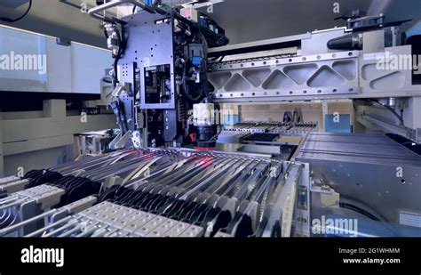
Automated PCBA tools, like pick-and-place machines, rely on precise CAD data to achieve accuracy. However, manual reviews remain essential to verify clearances and alignment. By balancing automated efficiency with human oversight, engineers ensure flawless PCB assembly while paving the way for reliable soldering and testing phases.
Precision Soldering for Reliable PCBs
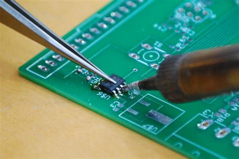
Achieving flawless PCB assembly hinges on mastering precision soldering techniques, which directly impact electrical connectivity and long-term durability. Whether using manual or automated processes, maintaining optimal solder joint quality is non-negotiable. For PCBA success, temperature control is critical—excessive heat risks damaging components, while insufficient heat leads to cold joints. Modern reflow ovens with programmable profiles ensure consistent thermal management, especially for surface-mount devices (SMDs).
Hand-soldering remains vital for prototyping or delicate components, demanding skilled technicians to apply flux and solder wire with micron-level accuracy. Automated systems, however, excel in high-volume production, leveraging robotic arms and vision systems to place and solder components within ±0.1mm tolerances. As explored in this comparison, hybrid approaches often yield the best results, blending speed with human oversight.
Post-soldering inspection—via automated optical inspection (AOI) or X-ray—identifies defects like bridging or voids. Properly executed soldering not only ensures electrical integrity but also mitigates thermal stress, a common failure point in PCB assembly. By prioritizing precision at this stage, manufacturers lay the groundwork for reliable PCBs that withstand rigorous operational demands.
Advanced PCB Testing for Durability
Rigorous testing protocols are essential to ensure the long-term durability of PCB assembly (PCBA) in demanding environments. After component placement and soldering, advanced tests simulate real-world stressors—such as thermal cycling, vibration, and humidity exposure—to identify potential weaknesses. Automated optical inspection (AOI) and X-ray imaging play pivotal roles in detecting micro-cracks, solder voids, or misaligned components that could compromise structural integrity. For high-reliability applications, environmental stress screening (ESS) subjects assembled boards to extreme temperatures and mechanical shocks, validating performance under harsh conditions.
Electrical testing, including in-circuit testing (ICT) and functional testing, verifies signal integrity and power distribution, ensuring every trace and connection meets design specifications. Incorporating boundary scan testing further isolates faults in complex circuits, reducing debugging time post-assembly. By integrating these methods into the PCBA workflow, manufacturers preemptively address failure points, extending the operational lifespan of electronic systems. Transitioning seamlessly from design validation to final quality assurance, these tests form the backbone of reliable PCB assembly, aligning with industry standards for aerospace, automotive, and medical devices.

PCB Assembly Quality Control Steps
Effective PCB assembly quality control begins with rigorous inspection protocols to identify defects early. Automated Optical Inspection (AOI) systems scan solder joints and component placements for misalignments, bridging, or insufficient solder. For high-density boards, X-ray inspection verifies hidden connections, such as ball grid arrays (BGAs), ensuring structural integrity. Post-soldering, electrical testing validates circuit continuity and functionality, while environmental stress tests—like thermal cycling—assess durability under extreme conditions.
To maintain consistency, statistical process control (SPC) tracks production metrics, flagging deviations in real time. Partnering with certified PCBA providers ensures adherence to industry standards like IPC-A-610, which defines acceptability criteria for PCB assembly. Cross-functional reviews between design and manufacturing teams further refine tolerances, minimizing rework. Finally, documentation audits guarantee traceability, critical for compliance in aerospace or medical applications. By integrating these steps, manufacturers achieve zero-defect outcomes, balancing precision with scalability across production batches.
Expert Tips for Flawless PCB Assembly
Achieving precision in PCB assembly requires a blend of technical expertise and meticulous attention to detail. Start by verifying component orientation and footprint compatibility during placement, as even minor mismatches can lead to catastrophic failures. Use PCBA-specific tools like pick-and-place machines to ensure consistent alignment, especially for surface-mount devices (SMDs). While soldering, maintain a controlled temperature profile to prevent thermal stress—excessive heat risks damaging sensitive components, while insufficient heat creates weak joints.
Another critical aspect is flux management. High-quality no-clean flux minimizes residue, reducing the risk of corrosion in long-term applications. For through-hole components, ensure solder wicking fully covers leads without creating bridges. Post-soldering, employ automated optical inspection (AOI) systems to detect hidden defects like micro-cracks or insufficient solder.
Don’t overlook environmental factors. Static discharge can compromise PCBA integrity, so always work in an ESD-safe zone. Additionally, store moisture-sensitive components in dry cabinets to prevent oxidation. Finally, document every step meticulously—traceability is key for troubleshooting and quality assurance. By integrating these practices, you’ll enhance the reliability and longevity of assembled boards, aligning with industry standards for high-performance PCB assembly.
Optimizing PCB Layouts for Performance
Effective PCB assembly begins with strategic layout design, as even minor errors in component arrangement or trace routing can compromise functionality. Signal integrity and thermal management are pivotal considerations when optimizing layouts for high-performance PCBA. Start by grouping components based on their functional relationships and power requirements—placing sensitive analog circuits away from noisy digital sections minimizes interference.
Trace width and spacing must align with current-carrying capacity and impedance control needs, particularly for high-frequency applications. Utilizing ground planes and proper via placement enhances electromagnetic compatibility (EMC) while reducing crosstalk. Thermal vias and copper pours near heat-generating components, such as voltage regulators, prevent localized overheating that could degrade solder joints over time.
Modern design tools enable simulation of PCB assembly outcomes, allowing engineers to predict thermal hotspots or signal delays before prototyping. Adhering to Design for Manufacturability (DFM) guidelines—such as maintaining adequate clearance for automated pick-and-place machines—ensures seamless transition from design to PCBA production. By balancing electrical performance with manufacturability, optimized layouts lay the foundation for reliable, long-lasting circuit boards ready for rigorous testing phases.
Ensuring PCB Reliability Through Testing
Thorough testing is the cornerstone of achieving long-term reliability in PCB assembly processes. After components are placed and soldered, systematic validation ensures that every PCBA meets stringent performance criteria. In-Circuit Testing (ICT) verifies electrical connectivity and component functionality, while functional testing simulates real-world operating conditions to identify potential failures. For high-density boards, Automated Optical Inspection (AOI) complements these methods by detecting soldering defects or misaligned components with micron-level precision.
Environmental stress tests, such as thermal cycling and vibration testing, further validate durability under extreme conditions—a critical step for applications in aerospace or industrial automation. To maintain consistency, statistical process control (SPC) tools analyze test data, enabling rapid adjustments in manufacturing workflows. For teams collaborating across locations, remote monitoring tools provide real-time insights into testing metrics, ensuring alignment with design specifications.
By integrating these protocols early in the PCB assembly lifecycle, manufacturers minimize rework costs and deliver PCBA products that balance precision, repeatability, and interoperability with downstream systems. This proactive approach not only safeguards performance but also strengthens compliance with industry certifications like IPC-A-610.
Conclusion
Achieving flawless PCB assembly requires meticulous attention to every stage of the process, from design validation to final testing. By prioritizing precision in component placement and adhering to industry-standard soldering techniques, manufacturers can minimize defects and enhance the longevity of PCBA products. Rigorous quality control protocols, including automated optical inspection (AOI) and functional testing, ensure that each board meets performance benchmarks while identifying potential failures early.
To maintain consistency, integrating design-for-manufacturability (DFM) principles during layout optimization reduces risks associated with thermal management and signal integrity. Partnering with trusted experts, such as Gold Phoenix PCB, provides access to advanced tools and specialized knowledge for complex projects. Ultimately, the synergy between skilled craftsmanship, cutting-edge technology, and thorough validation processes forms the foundation of reliable PCB assembly outcomes. By embracing these practices, engineers and manufacturers can deliver durable, high-performance electronics that withstand evolving industry demands.
FAQs
What are the most common mistakes to avoid during PCB assembly?
Improper component placement and inadequate solder paste application often lead to failures. Ensuring precise alignment and avoiding thermal stress during soldering are critical. Overlooking PCB testing protocols, such as automated optical inspection (AOI), can also compromise reliability.
How does component placement impact PCB performance?
Optimal component placement minimizes signal interference and heat buildup. Strategic positioning of high-power components away from sensitive circuits enhances electrical performance and durability. This step directly affects PCBA functionality and long-term stability.
What soldering techniques ensure reliable PCB connections?
Reflow soldering is ideal for surface-mount components, while wave soldering suits through-hole parts. Using lead-free solder with controlled temperature profiles prevents cold joints and ensures robust connections in PCB assembly.
Why is testing crucial after assembling PCBs?
Advanced PCB testing identifies latent defects like short circuits or open traces. Techniques like in-circuit testing (ICT) and functional testing validate PCBA performance under real-world conditions, preventing costly field failures.
How can manufacturers maintain consistency in PCB quality?
Implementing quality control steps such as X-ray inspection and electrical stress testing ensures uniformity. Adhering to IPC-A-610 standards during PCB assembly guarantees compliance with industry benchmarks.