Flex pcb bonding
Advantages Of Flex PCB Bonding In Modern Electronics
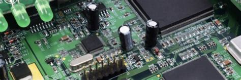
Flex PCB bonding has emerged as a pivotal technology in the realm of modern electronics, offering a multitude of advantages that cater to the ever-evolving demands of the industry. As electronic devices continue to shrink in size while expanding in functionality, the need for more efficient and reliable circuit solutions becomes increasingly apparent. Flex PCBs, or flexible printed circuit boards, provide a versatile and innovative approach to meeting these requirements, primarily through their unique bonding capabilities.
One of the foremost advantages of flex PCB bonding is its ability to accommodate complex and compact designs.
Unlike traditional rigid PCBs, flex PCBs can be bent, folded, and twisted to fit into tight spaces, making them ideal for applications where space is at a premium. This flexibility allows designers to create intricate circuits that can conform to the contours of various devices, from wearable technology to advanced medical equipment. Consequently, the adaptability of flex PCB bonding facilitates the development of smaller, lighter, and more efficient electronic products.
In addition to their spatial efficiency, flex PCBs offer enhanced durability and reliability.
The bonding process used in flex PCBs typically involves the use of advanced adhesives and materials that can withstand a wide range of environmental conditions. This resilience is particularly beneficial in applications where the electronic components are subject to mechanical stress, temperature fluctuations, or exposure to moisture. By maintaining their integrity under such conditions, flex PCBs ensure consistent performance and longevity, which is crucial for both consumer electronics and industrial applications.
Moreover, the thermal management capabilities of flex PCB bonding are noteworthy.
As electronic devices become more powerful, they generate more heat, which can adversely affect performance and lifespan. Flex PCBs, with their ability to dissipate heat effectively, help mitigate these issues. The materials used in flex PCB bonding often possess excellent thermal conductivity, allowing heat to be distributed evenly across the board. This characteristic not only enhances the performance of the device but also contributes to its overall reliability and safety.
Another significant advantage of flex PCB bonding is its contribution to cost efficiency in manufacturing.
The streamlined design and reduced material usage associated with flex PCBs can lead to lower production costs. Additionally, the ability to integrate multiple components into a single flex PCB reduces the need for additional connectors and interconnections, further simplifying the assembly process. This reduction in complexity not only decreases manufacturing time but also minimizes the potential for errors, resulting in higher yields and lower defect rates.
Furthermore, the environmental benefits of flex PCB bonding should not be overlooked.
The reduced material usage and energy consumption during production align with the growing emphasis on sustainable manufacturing practices. As industries strive to minimize their environmental footprint, the adoption of flex PCBs represents a step towards more eco-friendly electronic solutions.
In conclusion, the advantages of flex PCB bonding in modern electronics are manifold, encompassing design flexibility, durability, thermal management, cost efficiency, and environmental sustainability. As technology continues to advance, the role of flex PCBs is likely to expand, driving innovation and enabling the development of next-generation electronic devices. By embracing the capabilities of flex PCB bonding, manufacturers can not only meet the current demands of the market but also anticipate and adapt to future challenges in the ever-evolving landscape of electronics.
Techniques For Effective Flex PCB Bonding
Flex PCB bonding is a critical process in the manufacturing of flexible printed circuit boards, which are increasingly used in a variety of applications due to their lightweight, compact, and versatile nature. As the demand for more sophisticated electronic devices grows, the need for effective bonding techniques becomes paramount. Understanding the nuances of these techniques is essential for ensuring the reliability and performance of flex PCBs.
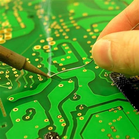
To begin with, one of the most common techniques for flex PCB bonding is the use of adhesive materials.
Adhesives are selected based on their ability to withstand environmental stresses such as temperature fluctuations, humidity, and mechanical strain. Epoxy-based adhesives are frequently used due to their strong bonding properties and resistance to harsh conditions. However, selecting the appropriate adhesive requires careful consideration of the specific application and the materials involved in the PCB construction.
In addition to adhesives, thermal bonding is another widely used technique.
This method involves the application of heat and pressure to bond layers of the flex PCB together. The process is often carried out using specialized equipment such as hot bar soldering machines or thermal bonding presses. The advantage of thermal bonding lies in its ability to create a strong, uniform bond across the entire surface area, which is crucial for maintaining the integrity of the circuit under dynamic conditions. However, it is important to control the temperature and pressure precisely to avoid damaging the delicate components of the PCB.
Moreover, ultrasonic bonding is gaining popularity as an effective technique for flex PCB bonding.
This method utilizes high-frequency ultrasonic vibrations to generate heat at the interface of the materials being bonded. The localized heating effect allows for precise bonding without the need for external heat sources, making it ideal for applications where thermal sensitivity is a concern. Ultrasonic bonding is particularly advantageous for joining dissimilar materials, as it can create strong bonds without the need for additional adhesives.
Furthermore, laser bonding is an emerging technique that offers high precision and control.
By using a focused laser beam, this method can selectively bond specific areas of the flex PCB, allowing for intricate designs and complex circuitry. The non-contact nature of laser bonding minimizes the risk of mechanical damage, making it suitable for delicate and miniaturized components. However, the implementation of laser bonding requires sophisticated equipment and expertise, which can be a limiting factor for some manufacturers.
In addition to these techniques, it is essential to consider the design and layout of the flex PCB during the bonding process.
Proper design can significantly enhance the effectiveness of the bonding techniques employed. For instance, incorporating features such as strain reliefs and appropriate pad sizes can help distribute mechanical stresses more evenly, reducing the likelihood of bond failure. Additionally, ensuring that the surfaces to be bonded are clean and free from contaminants is crucial for achieving optimal adhesion.
In conclusion, the choice of bonding technique for flex PCBs depends on various factors, including the materials involved, the intended application, and the specific requirements of the device. By understanding the advantages and limitations of each technique, manufacturers can make informed decisions that enhance the performance and reliability of their products. As technology continues to advance, ongoing research and development in flex PCB bonding techniques will undoubtedly lead to even more innovative solutions in the future.
Common Challenges In Flex PCB Bonding And How To Overcome Them
Flex PCB bonding is a critical process in the manufacturing of flexible printed circuit boards, which are increasingly used in a variety of applications due to their lightweight, compact, and versatile nature. However, this process is not without its challenges. Understanding these challenges and how to effectively address them is essential for ensuring the reliability and performance of the final product.
One of the primary challenges in flex PCB bonding is achieving a strong and reliable bond between the flexible substrate and the components.
This difficulty often arises due to the inherent properties of the materials involved. Flexible substrates, typically made from polyimide or polyester, have different thermal expansion coefficients compared to the components being attached. This discrepancy can lead to stress and potential delamination during thermal cycling. To overcome this, manufacturers can employ advanced adhesive materials specifically designed to accommodate these differences in thermal expansion. These adhesives not only provide strong bonding but also maintain flexibility, which is crucial for the dynamic environments in which flex PCBs are often used.
Another significant challenge is the alignment of components during the bonding process.
Flex PCBs are often used in applications where space is at a premium, necessitating precise placement of components. Misalignment can lead to electrical failures or reduced performance. To address this issue, manufacturers can utilize automated optical inspection systems that ensure components are accurately placed before bonding. Additionally, employing fiducial markers on the PCB can aid in the precise alignment of components, thereby reducing the risk of misalignment.
The bonding process itself can also present challenges, particularly in terms of temperature and pressure control.
Excessive heat or pressure can damage the delicate flexible substrate, while insufficient heat or pressure may result in weak bonds. To mitigate these risks, it is essential to carefully control the bonding parameters. Utilizing equipment with precise temperature and pressure controls can help achieve the optimal conditions for bonding. Moreover, conducting thorough testing and validation of the bonding process can ensure that the parameters are correctly set for each specific application.
Contamination is another issue that can compromise the integrity of flex PCB bonds.
Dust, oils, and other contaminants can interfere with the adhesion process, leading to weak or unreliable bonds. To prevent contamination, it is crucial to maintain a clean manufacturing environment. Implementing cleanroom standards and using anti-static materials can significantly reduce the risk of contamination. Additionally, proper handling procedures should be established to minimize the introduction of contaminants during the manufacturing process.
Finally, the mechanical flexibility of flex PCBs, while advantageous, can also pose challenges during bonding.
The bending and flexing that these boards undergo can place additional stress on the bonds, potentially leading to failure over time. To address this, manufacturers can design the PCB layout to minimize stress concentrations and use strain relief techniques to distribute mechanical loads more evenly across the board. Furthermore, selecting adhesives with high flexibility and fatigue resistance can enhance the durability of the bonds under repeated flexing.
In conclusion, while flex PCB bonding presents several challenges, understanding these issues and implementing appropriate strategies can significantly improve the reliability and performance of flexible printed circuit boards. By carefully selecting materials, controlling the bonding process, maintaining a clean environment, and designing for mechanical flexibility, manufacturers can overcome these challenges and produce high-quality flex PCBs that meet the demands of modern applications.
Innovations In Flex PCB Bonding Technology
Flex PCB bonding technology has undergone significant advancements in recent years, driven by the increasing demand for more compact, efficient, and reliable electronic devices. As the electronics industry continues to evolve, the need for flexible printed circuit boards (PCBs) has become more pronounced, particularly in applications where space constraints and dynamic environments are prevalent. These applications range from consumer electronics to automotive and medical devices, where flexibility and durability are paramount. Consequently, innovations in flex PCB bonding technology have emerged as a critical area of focus, aiming to enhance performance while maintaining cost-effectiveness.
One of the most notable advancements in flex PCB bonding technology is the development of advanced adhesive materials.
These materials are designed to provide superior bonding strength while accommodating the flexibility required by modern electronic devices. Traditional bonding methods often faced challenges such as delamination and poor thermal management, which could compromise the integrity and functionality of the circuit. However, with the introduction of new adhesive formulations, these issues are being effectively addressed. These adhesives not only offer improved thermal conductivity but also exhibit excellent resistance to environmental factors such as moisture and temperature fluctuations, thereby extending the lifespan of the flex PCBs.
In addition to adhesive innovations, the integration of laser technology in flex PCB bonding processes has marked a significant leap forward.
Laser bonding techniques offer precision and control that are unmatched by conventional methods. By utilizing laser energy, manufacturers can achieve highly accurate and localized bonding, which is particularly beneficial for complex circuit designs with intricate patterns. This precision reduces the risk of damage to sensitive components and ensures a more reliable connection. Moreover, laser bonding is a non-contact process, which minimizes mechanical stress on the flex PCB, further enhancing its durability and performance.
Furthermore, the advent of automated bonding systems has revolutionized the production of flex PCBs.
Automation not only increases production efficiency but also ensures consistency and repeatability in the bonding process. Automated systems are equipped with advanced sensors and control mechanisms that monitor and adjust parameters in real-time, ensuring optimal bonding conditions. This level of control is crucial in maintaining the quality and reliability of the final product, especially in high-volume manufacturing environments where even minor deviations can lead to significant defects.
Another promising development in flex PCB bonding technology is the exploration of novel bonding techniques such as anisotropic conductive films (ACFs) and non-conductive films (NCFs).
These materials offer unique advantages in terms of electrical conductivity and mechanical stability. ACFs, for instance, allow for electrical connections to be made only in specific areas, reducing the risk of short circuits and improving overall circuit performance. On the other hand, NCFs provide robust mechanical support without compromising the electrical properties of the circuit, making them ideal for applications where mechanical stress is a concern.
In conclusion, the innovations in flex PCB bonding technology are paving the way for more advanced and reliable electronic devices. As the demand for flexible and durable electronics continues to grow, these technological advancements will play a crucial role in meeting the evolving needs of various industries. By leveraging new materials, precision techniques, and automation, manufacturers are not only enhancing the performance of flex PCBs but also ensuring their long-term viability in an increasingly competitive market. As research and development efforts continue, it is anticipated that further breakthroughs will emerge, driving the next generation of flex PCB bonding solutions.