Flex pcb fabrication notes
Design Guidelines For Flex PCB Fabrication notes
Flex PCB fabrication is a sophisticated process that requires meticulous attention to design guidelines to ensure optimal performance and reliability.
One of the primary considerations in designing flex PCBs is the material selection.
Polyimide is commonly used due to its excellent thermal stability, flexibility, and electrical properties. However, the choice of adhesive and copper foil also plays a crucial role in the overall performance of the flex PCB. It is essential to select materials that can withstand the mechanical stresses and environmental conditions the PCB will encounter.
Another critical aspect of flex PCB design is the layout of the traces.
To minimize stress and potential damage, traces should be routed with smooth, curved paths rather than sharp angles. This approach helps distribute mechanical stress more evenly across the flex PCB, reducing the likelihood of cracks or breaks. Additionally, maintaining a consistent trace width and spacing is vital to ensure signal integrity and prevent issues such as crosstalk or impedance mismatches.
The stack-up configuration is another important factor in flex PCB design.
A well-planned stack-up can significantly enhance the performance and reliability of the PCB. It is advisable to use symmetrical stack-ups to prevent warping and ensure even distribution of mechanical stress. Furthermore, incorporating stiffeners in areas that require additional support can help maintain the structural integrity of the flex PCB, especially in regions subjected to repeated bending or mechanical loads.
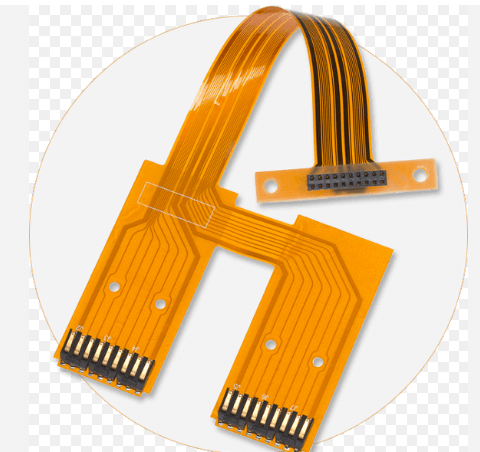
When designing flex PCBs, it is also crucial to consider the bend radius.
The bend radius is the minimum radius that the flex PCB can be bent without causing damage. A general rule of thumb is to maintain a bend radius of at least ten times the thickness of the flex PCB. This guideline helps prevent excessive stress on the copper traces and dielectric material, thereby enhancing the durability and longevity of the flex PCB.
Moreover, the placement of components on a flex PCB requires careful consideration.
Components should be positioned in areas that experience minimal mechanical stress to avoid potential damage during bending or flexing. It is also advisable to use surface-mount technology (SMT) components rather than through-hole components, as SMT components are generally more resilient to mechanical stress and provide a lower profile, which is beneficial for flexible applications.
Thermal management is another critical aspect of flex PCB design.
Due to the compact nature of flex PCBs, effective heat dissipation can be challenging. Incorporating thermal vias, heat sinks, and proper trace routing can help manage heat effectively. Additionally, selecting materials with good thermal conductivity can further enhance the thermal performance of the flex PCB.
In conclusion, designing flex PCBs requires a comprehensive understanding of various factors, including material selection, trace layout, stack-up configuration, bend radius, component placement, and thermal management. By adhering to these design guidelines, engineers can create flex PCBs that are not only reliable and durable but also capable of meeting the demanding requirements of modern electronic applications. The meticulous attention to detail in the design phase can significantly impact the performance and longevity of the final product, making it imperative to follow best practices and industry standards throughout the design and fabrication process.

Material Selection In Flex PCB Manufacturing
In the realm of flex PCB manufacturing, material selection plays a pivotal role in determining the performance, reliability, and longevity of the final product. The choice of materials directly impacts the flexibility, thermal stability, and electrical properties of the flexible printed circuit boards (PCBs). Therefore, understanding the nuances of material selection is essential for engineers and designers aiming to optimize their flex PCB designs.
To begin with, the base material, or substrate, is a critical component in flex PCB fabrication.
Polyimide is the most commonly used substrate due to its excellent thermal stability, mechanical strength, and flexibility. Polyimide substrates can withstand high temperatures, making them suitable for applications that require soldering and other high-temperature processes. Additionally, polyimide’s inherent flexibility allows it to bend and twist without compromising the integrity of the circuit, which is essential for applications in wearable electronics, medical devices, and aerospace technologies.
Another important material in flex PCB manufacturing is the adhesive system used to bond the layers of the PCB.
The adhesive must provide strong adhesion while maintaining flexibility and thermal stability. Acrylic and epoxy adhesives are frequently used in flex PCB fabrication. Acrylic adhesives offer good flexibility and are suitable for dynamic flex applications where the PCB will be subjected to repeated bending. On the other hand, epoxy adhesives provide superior thermal stability and chemical resistance, making them ideal for applications exposed to harsh environments.
The choice of conductive materials is equally significant in flex PCB manufacturing.
Copper is the preferred conductive material due to its excellent electrical conductivity and ductility. Copper can be deposited on the substrate using various methods, including electroplating and laminating copper foil. The thickness of the copper layer must be carefully selected to balance conductivity and flexibility. Thicker copper layers provide lower electrical resistance but may reduce the flexibility of the PCB. Conversely, thinner copper layers enhance flexibility but may increase electrical resistance.
In addition to the primary materials, protective coatings and surface finishes are crucial in flex PCB fabrication.
Protective coatings, such as solder masks and coverlays, shield the circuit from environmental factors like moisture, dust, and chemicals. Polyimide coverlays are commonly used due to their compatibility with the polyimide substrate and their ability to withstand high temperatures. Surface finishes, such as immersion gold or silver, are applied to the exposed copper pads to enhance solderability and protect against oxidation.
Furthermore, the mechanical properties of the materials must be considered to ensure the durability of the flex PCB.
The materials should exhibit high tensile strength and elongation to withstand mechanical stresses during installation and operation. The coefficient of thermal expansion (CTE) of the materials should be matched to minimize thermal stress during temperature fluctuations.
In conclusion, material selection in flex PCB manufacturing is a multifaceted process that requires careful consideration of various factors, including thermal stability, flexibility, electrical conductivity, and mechanical properties. By selecting the appropriate materials, engineers and designers can create flex PCBs that meet the specific requirements of their applications, ensuring optimal performance and reliability. The interplay of these materials ultimately defines the success of the flex PCB, making material selection a cornerstone of the manufacturing process.
Common Challenges In Flex PCB Fabrication
Flex PCB fabrication, while offering numerous advantages such as flexibility, space savings, and improved reliability, presents a unique set of challenges that must be meticulously managed to ensure successful outcomes.
One of the primary challenges in flex PCB fabrication is material selection.
The materials used in flex PCBs, such as polyimide films and adhesive systems, must possess specific properties to withstand the mechanical stresses and environmental conditions they will encounter. Selecting the wrong materials can lead to issues such as delamination, cracking, or inadequate thermal performance, which can compromise the functionality and longevity of the final product.
Another significant challenge is the design complexity inherent in flex PCBs.
Unlike rigid PCBs, flex PCBs must be designed to accommodate bending and flexing without causing damage to the conductive traces or the substrate. This requires careful consideration of factors such as bend radius, trace width, and the placement of components. Designers must also account for the dynamic mechanical stresses that the flex PCB will experience during its operational life, which can be particularly challenging in applications that involve repeated flexing or movement.
Manufacturing precision is also a critical concern in flex PCB fabrication.
The thin and flexible nature of the materials used can make them more susceptible to handling damage and manufacturing defects. For instance, the drilling process must be carefully controlled to avoid tearing or distorting the substrate. Similarly, the etching process must be precisely managed to ensure that the conductive traces are accurately formed without over-etching or under-etching. Any deviations in these processes can lead to electrical failures or reduced performance.
Furthermore, the assembly process for flex PCBs can be more complex than for rigid PCBs.
The flexible nature of the substrate can make it more difficult to align and place components accurately. Additionally, the soldering process must be carefully controlled to avoid damaging the substrate or causing warping. This often requires specialized equipment and techniques, such as the use of low-temperature soldering processes or the application of stiffeners to provide temporary rigidity during assembly.
Quality control is another area where flex PCB fabrication presents unique challenges.
The thin and flexible materials used in flex PCBs can make it more difficult to detect defects using traditional inspection methods. Advanced inspection techniques, such as automated optical inspection (AOI) and X-ray inspection, are often required to ensure that the flex PCBs meet the necessary quality standards. These techniques can add to the overall cost and complexity of the fabrication process.
In addition to these technical challenges, there are also logistical considerations that must be managed.
The supply chain for the specialized materials used in flex PCBs can be more complex and less predictable than for rigid PCBs. This can lead to longer lead times and increased costs, particularly for high-performance materials that are not widely available. Effective supply chain management is therefore essential to ensure that the necessary materials are available when needed and that the fabrication process can proceed without delays.
In conclusion, while flex PCB fabrication offers significant advantages, it also presents a range of challenges that must be carefully managed.
From material selection and design complexity to manufacturing precision and quality control, each step in the process requires careful attention to detail and specialized knowledge. By understanding and addressing these challenges, manufacturers can ensure that their flex PCBs meet the necessary performance and reliability standards, enabling them to take full advantage of the benefits that this technology offers.
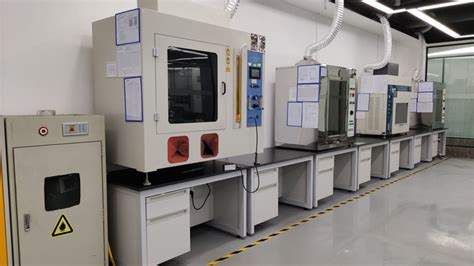
Quality Control Measures In Flex PCB Production
Quality control measures in flex PCB production are critical to ensuring the reliability and performance of the final product. The process begins with the selection of high-quality raw materials, as the foundation of any robust flex PCB lies in the materials used. Polyimide films, copper foils, and adhesives must meet stringent specifications to withstand the mechanical and thermal stresses encountered during both manufacturing and operation. Once the materials are procured, they undergo rigorous inspection to verify their conformity to industry standards.
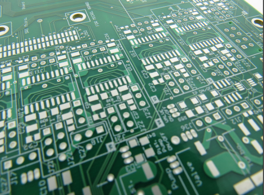
Following material inspection, the next step involves precise imaging and etching processes.
Photolithography is employed to transfer the circuit design onto the copper-clad polyimide film. This step requires meticulous attention to detail, as any deviation can lead to circuit failures. To ensure accuracy, advanced imaging systems are used to align the photomask with the substrate. Post-imaging, the etching process removes unwanted copper, leaving behind the desired circuit pattern. Quality control at this stage includes inspecting the etched circuits for defects such as undercutting, over-etching, or incomplete etching, which can compromise the electrical integrity of the PCB.
Subsequently, the drilled holes, or vias, which facilitate electrical connections between different layers of the PCB, are created.
Laser drilling is often preferred for its precision and ability to create small, clean holes. The quality of these vias is critical, as any misalignment or irregularity can lead to poor electrical connections. Therefore, automated optical inspection (AOI) systems are employed to verify the accuracy and quality of the drilled holes.
The next phase involves the application of a protective solder mask and surface finish.
The solder mask prevents solder bridges during component assembly and protects the copper traces from oxidation and environmental damage. The application process must be uniform and free from defects such as bubbles or voids. Quality control measures include visual inspection and thickness measurement to ensure consistent coverage. The surface finish, typically applied through processes like electroless nickel immersion gold (ENIG) or hot air solder leveling (HASL), provides a solderable surface for component attachment. The finish must be smooth and uniform to ensure reliable solder joints.
Electrical testing is another crucial quality control measure in flex PCB production.
This involves subjecting the PCB to various electrical tests to verify continuity and isolation of the circuits. Flying probe testers or bed-of-nails fixtures are commonly used for this purpose. These tests help identify open circuits, short circuits, and other electrical faults that could affect the performance of the final product.
Finally, the assembled flex PCBs undergo a series of environmental and mechanical tests to simulate real-world operating conditions.
These tests include thermal cycling, humidity exposure, and flexural endurance tests. The goal is to ensure that the PCBs can withstand the stresses they will encounter in their intended applications. Any failures during these tests are analyzed to identify root causes and implement corrective actions.
In conclusion, quality control measures in flex PCB production are multifaceted and encompass every stage of the manufacturing process. From material selection and imaging to drilling, solder mask application, electrical testing, and environmental simulation, each step is meticulously monitored to ensure the highest standards of quality and reliability. These measures are essential to producing flex PCBs that meet the rigorous demands of modern electronic applications.