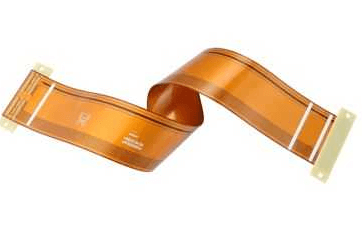
Flex pcb folding
Advantages Of Flex PCB Folding In Modern Electronics
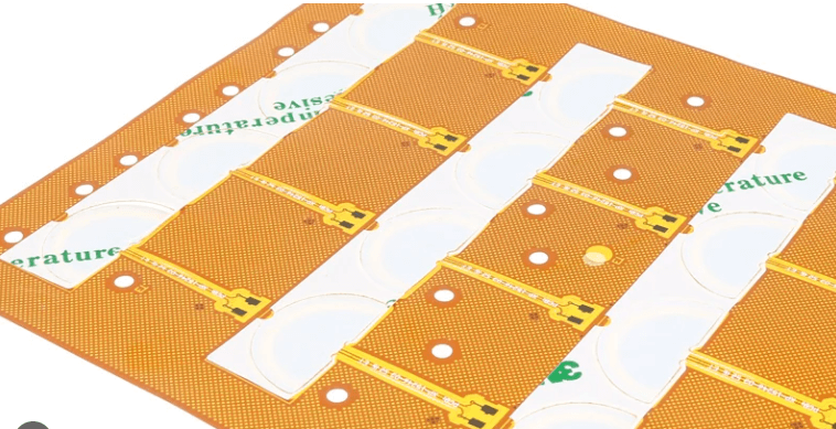
Flex PCB folding, a technique that involves bending flexible printed circuit boards (PCBs) to fit into compact spaces, has become increasingly advantageous in the realm of modern electronics. As devices continue to shrink in size while expanding in functionality, the demand for innovative solutions to accommodate complex circuitry within limited spaces has grown. Flex PCB folding emerges as a pivotal solution, offering numerous benefits that enhance the design and performance of contemporary electronic devices.
One of the primary advantages of flex PCB folding is its ability to significantly reduce the size and weight of electronic devices.
Traditional rigid PCBs often require additional connectors and cables to link different components, which can add bulk and complexity. In contrast, flex PCBs can be folded or bent to fit into tight spaces, eliminating the need for extra connectors and reducing the overall footprint of the device. This capability is particularly beneficial in the design of portable electronics, such as smartphones, tablets, and wearable devices, where space is at a premium and weight reduction is crucial for user comfort and device portability.
Moreover, flex PCB folding enhances the reliability and durability of electronic devices.
The flexibility of these PCBs allows them to absorb mechanical stresses and vibrations that would otherwise damage rigid boards. This resilience is especially important in applications where devices are subject to frequent movement or harsh environmental conditions, such as in automotive or aerospace industries. By minimizing the risk of mechanical failure, flex PCB folding contributes to the longevity and dependability of electronic products.
In addition to size reduction and durability, flex PCB folding offers significant design flexibility.
Engineers can create complex three-dimensional configurations that would be impossible with rigid PCBs. This freedom in design enables the development of innovative product shapes and functionalities, pushing the boundaries of what is possible in electronic design. For instance, in medical devices, where intricate and compact designs are often required, flex PCB folding allows for the integration of advanced features without compromising on size or performance.
Furthermore, the use of flex PCB folding can lead to cost savings in the manufacturing process.
By reducing the number of components and interconnections needed, manufacturers can streamline assembly processes and reduce material costs. Additionally, the ability to fold and fit PCBs into smaller spaces can lead to more efficient use of materials, further driving down production expenses. These cost benefits are particularly appealing in industries where large-scale production and cost efficiency are critical to maintaining competitive advantage.
Despite these advantages, it is important to acknowledge that flex PCB folding does present some challenges.
The design and manufacturing processes require specialized skills and equipment, which can initially increase development time and costs. However, as technology advances and expertise in this area grows, these challenges are becoming less prohibitive, making flex PCB folding an increasingly viable option for a wide range of applications.
In conclusion, the advantages of flex PCB folding in modern electronics are manifold, encompassing size and weight reduction, enhanced reliability, design flexibility, and cost efficiency. As the demand for smaller, more powerful electronic devices continues to rise, the role of flex PCB folding in meeting these demands is likely to expand, driving further innovation and development in the field of electronics.

Techniques For Effective Flex PCB Folding
Flex PCB folding is a critical technique in the design and implementation of flexible printed circuit boards, which are increasingly utilized in modern electronic devices due to their adaptability and space-saving capabilities. As electronic devices become more compact and complex, the demand for efficient and reliable flex PCB folding techniques has grown significantly. Understanding the principles and methods of effective flex PCB folding is essential for engineers and designers aiming to optimize the performance and durability of these circuits.
To begin with, it is important to recognize that flex PCBs are designed to bend and fold without compromising their functionality.
This inherent flexibility allows them to fit into tight spaces and conform to the contours of various devices. However, improper folding can lead to mechanical stress, which may cause circuit failure. Therefore, one of the primary techniques for effective flex PCB folding is to ensure that the bending radius is within the material’s tolerance limits. The bending radius is the minimum radius that a flex PCB can be bent without causing damage. Adhering to the recommended bending radius helps prevent stress fractures and maintains the integrity of the circuit.
In addition to considering the bending radius, another crucial technique involves the strategic placement of components.
Components should be positioned in such a way that they do not interfere with the folding process. This often means placing components away from the fold lines or using smaller components that can withstand the mechanical stress of bending. Furthermore, it is advisable to use flexible components, such as surface-mount devices, which are less likely to be damaged during folding.
Moreover, the choice of materials plays a significant role in the effectiveness of flex PCB folding.
Materials with high flexibility and durability, such as polyimide, are preferred for their ability to withstand repeated bending without degradation. Additionally, the use of adhesive materials that can endure mechanical stress is essential to maintain the structural integrity of the folded PCB. By selecting appropriate materials, designers can enhance the longevity and reliability of the flex PCB.
Another technique involves the use of reinforcement in areas that are subject to frequent bending.
Reinforcement can be achieved through the application of stiffeners, which are additional layers of material that provide extra support to the flex PCB. Stiffeners help distribute mechanical stress more evenly, reducing the likelihood of damage. However, it is important to balance the use of stiffeners with the need for flexibility, as excessive reinforcement can limit the PCB’s ability to bend.

Furthermore, simulation and testing are indispensable techniques in the development of effective flex PCB folding strategies.
By using computer-aided design (CAD) software, engineers can simulate the folding process and identify potential stress points. This allows for adjustments to be made before the physical prototype is created, saving time and resources. Once a prototype is developed, rigorous testing under various conditions ensures that the flex PCB can withstand the demands of its intended application.
In conclusion, effective flex PCB folding requires a comprehensive understanding of the material properties, component placement, and reinforcement techniques. By adhering to best practices and utilizing advanced simulation tools, designers can create flexible circuits that meet the demands of modern electronic devices. As technology continues to evolve, the importance of mastering flex PCB folding techniques will only increase, making it a vital skill for engineers and designers in the electronics industry.
Common Challenges In Flex PCB Folding And How To Overcome Them
Flex PCB folding is a critical process in the manufacturing of flexible printed circuit boards, which are increasingly used in modern electronic devices due to their ability to fit into compact spaces and conform to various shapes. However, this process is not without its challenges. Understanding these challenges and how to overcome them is essential for ensuring the reliability and performance of the final product.
One of the primary challenges in flex PCB folding is maintaining the integrity of the circuit during the folding process.
Flex PCBs are designed to be bent and folded, but excessive stress can lead to micro-cracks in the conductive traces or delamination of the layers. To mitigate this risk, it is crucial to design the PCB with appropriate bend radii. The bend radius should be at least ten times the thickness of the flex PCB to prevent damage. Additionally, using materials with high flexibility and durability, such as polyimide, can help withstand the mechanical stresses involved in folding.
Another significant challenge is the potential for signal integrity issues.
As flex PCBs are folded, the physical changes can affect the electrical characteristics of the circuit, leading to issues such as impedance mismatches and signal loss. To address this, careful attention must be paid to the layout and routing of the traces. Ensuring that the traces are routed in a way that minimizes changes in impedance is crucial. Moreover, incorporating ground planes and using controlled impedance techniques can help maintain signal integrity throughout the folding process.
Thermal management is also a concern when dealing with flex PCB folding.
The folding process can create hotspots, which may lead to overheating and, consequently, failure of the electronic components. To overcome this, it is important to design the PCB with adequate thermal management strategies. This can include the use of thermal vias, heat sinks, and appropriate spacing between components to facilitate heat dissipation. Additionally, selecting materials with good thermal conductivity can help manage heat more effectively.
Furthermore, the assembly process poses its own set of challenges.
The flexibility of the PCB can make it difficult to handle and assemble, leading to potential misalignments and defects. To mitigate these issues, it is advisable to use fixtures and supports during the assembly process to hold the PCB in place. Automated assembly equipment specifically designed for handling flexible circuits can also improve precision and reduce the risk of errors.
Finally, testing and inspection of flex PCBs can be more complex compared to rigid PCBs.
The flexible nature of these circuits can make it challenging to perform standard testing procedures. To address this, specialized testing equipment that can accommodate the flexibility of the PCB is necessary. Non-destructive testing methods, such as X-ray inspection and automated optical inspection, can be employed to ensure the integrity and functionality of the folded PCB without causing damage.
In conclusion, while flex PCB folding presents several challenges, these can be effectively managed through careful design, material selection, and process optimization. By understanding the potential issues and implementing strategies to address them, manufacturers can ensure the production of reliable and high-performance flex PCBs that meet the demands of modern electronic applications.
Innovations In Flex PCB Folding For Compact Device Design
In the rapidly evolving landscape of electronic device design, the demand for compact and efficient solutions has never been greater.
One of the most significant innovations addressing this need is the development of flexible printed circuit boards (PCBs), which have revolutionized the way electronic components are integrated into modern devices. Flex PCBs, characterized by their ability to bend and fold, offer a versatile alternative to traditional rigid circuit boards, enabling designers to create more compact and intricate device architectures. As the technology continues to advance, innovations in flex PCB folding are playing a crucial role in pushing the boundaries of what is possible in compact device design.
The primary advantage of flex PCBs lies in their inherent flexibility, which allows them to be folded or bent to fit into tight spaces within a device.
This capability is particularly beneficial in the design of wearable technology, smartphones, and other portable electronics, where space is at a premium. By utilizing flex PCBs, designers can optimize the internal layout of a device, reducing its overall size without compromising functionality. Moreover, the ability to fold these circuits enables the creation of multi-layered configurations, further enhancing the potential for miniaturization.
Recent advancements in materials science have significantly contributed to the evolution of flex PCB folding techniques.
The development of new, more durable materials has improved the reliability and longevity of flex PCBs, even when subjected to repeated bending and folding. These materials, often composed of polyimide or polyester films, provide excellent thermal stability and mechanical strength, ensuring that the circuits maintain their integrity under various environmental conditions. As a result, devices incorporating flex PCBs can achieve higher performance standards while maintaining a compact form factor.
In addition to material improvements, innovative manufacturing processes have also played a pivotal role in advancing flex PCB folding capabilities.
Techniques such as laser cutting and precision etching allow for the creation of intricate circuit patterns with high accuracy, enabling more complex folding configurations. These processes not only enhance the design flexibility of flex PCBs but also contribute to reducing production costs and time, making them an attractive option for manufacturers seeking efficient solutions for compact device design.
Furthermore, the integration of advanced simulation and modeling tools has facilitated the optimization of flex PCB folding designs.
By employing sophisticated software, engineers can predict the behavior of flex PCBs under various folding scenarios, allowing them to identify potential stress points and optimize the design accordingly. This predictive capability ensures that the final product is both reliable and efficient, meeting the stringent demands of modern electronic devices.
As the demand for smaller and more powerful devices continues to grow, the importance of innovations in flex PCB folding cannot be overstated. The ability to create compact, efficient, and reliable electronic components is essential for the development of next-generation technologies. By leveraging advancements in materials, manufacturing processes, and simulation tools, designers are now able to push the limits of what is possible, creating devices that are not only smaller but also more capable than ever before. In conclusion, the ongoing innovations in flex PCB folding are set to play a critical role in shaping the future of electronic device design, offering exciting possibilities for both manufacturers and consumers alike.