Flex pcb high speed
Design Considerations for High-Speed Flex PCBs
In the realm of modern electronics, the demand for compact, lightweight, and high-performance devices has led to the increased adoption of flexible printed circuit boards (PCBs). Among these, high-speed flex PCBs are particularly significant due to their ability to support rapid data transmission while maintaining flexibility and reliability. Designing high-speed flex PCBs, however, presents unique challenges that require careful consideration to ensure optimal performance and functionality.
To begin with, one of the primary considerations in designing high-speed flex PCBs is signal integrity.
As data rates increase, the potential for signal degradation becomes more pronounced. This degradation can manifest as signal loss, crosstalk, or electromagnetic interference (EMI), all of which can severely impact the performance of the circuit. To mitigate these issues, designers must pay close attention to the layout of the traces. Ensuring that traces are of uniform width and are spaced appropriately can help minimize impedance discontinuities, which are a common source of signal integrity problems.
Moreover, the choice of materials plays a crucial role in the performance of high-speed flex PCBs.
The dielectric constant and loss tangent of the substrate material can significantly affect signal propagation. Materials with a low dielectric constant and low loss tangent are preferred for high-speed applications as they reduce signal attenuation and dispersion. Polyimide is a popular choice for flex PCBs due to its excellent thermal stability and mechanical properties, but other advanced materials may be considered depending on the specific requirements of the application.
In addition to material selection, the stack-up configuration of the PCB is another critical factor.
A well-designed stack-up can help control impedance and reduce EMI. For high-speed applications, it is often beneficial to use a ground plane adjacent to the signal layers. This configuration not only provides a return path for signals, reducing loop area and thus EMI, but also helps maintain consistent impedance across the board. Furthermore, incorporating differential pairs for high-speed signals can enhance noise immunity and improve signal integrity.
Thermal management is another essential aspect of high-speed flex PCB design.
As data rates increase, so does the power consumption, leading to potential thermal issues. Effective thermal management strategies, such as the use of thermal vias, heat sinks, or thermal interface materials, can help dissipate heat and maintain the reliability of the PCB. Additionally, considering the thermal expansion properties of the materials used can prevent mechanical stress and potential failure of the board.
Transitioning to the mechanical design considerations, the flexibility of the PCB must be balanced with its electrical performance.
Bending and flexing can introduce mechanical stress, which may affect the reliability of the circuit. To address this, designers should consider the bend radius and the number of flex cycles the PCB will undergo during its lifetime. Reinforcing areas that are subject to frequent bending with stiffeners or using a thicker substrate can enhance durability without compromising flexibility.
Finally, manufacturing tolerances and process capabilities should not be overlooked.
High-speed flex PCBs often require tighter tolerances and more precise manufacturing processes than their rigid counterparts. Collaborating closely with manufacturers during the design phase can ensure that the design is feasible and that potential issues are addressed early on.
In conclusion, designing high-speed flex PCBs involves a complex interplay of electrical, thermal, and mechanical considerations. By carefully addressing these factors, designers can create PCBs that not only meet the demands of high-speed applications but also maintain the flexibility and reliability that are the hallmarks of flex PCBs.
Material Selection for Optimal Performance in High-Speed Flex PCBs
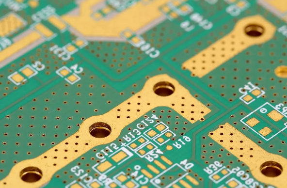
In the realm of high-speed flexible printed circuit boards (PCBs), material selection plays a pivotal role in determining the overall performance and reliability of the final product. As electronic devices continue to evolve, demanding faster data transmission rates and more compact designs, the need for high-speed flex PCBs has become increasingly critical. These advanced circuits are essential in applications ranging from consumer electronics to aerospace, where flexibility, lightweight, and high-speed capabilities are paramount. Therefore, understanding the intricacies of material selection is crucial for engineers and designers aiming to optimize the performance of high-speed flex PCBs.
To begin with, the dielectric material used in flex PCBs significantly influences signal integrity, especially at high frequencies.
Polyimide is a popular choice due to its excellent thermal stability, mechanical flexibility, and dielectric properties. However, for high-speed applications, the dielectric constant and loss tangent of the material must be carefully considered. A low dielectric constant is preferred as it reduces signal propagation delay, while a low loss tangent minimizes signal attenuation. Consequently, materials such as liquid crystal polymer (LCP) and polytetrafluoroethylene (PTFE) are often favored for their superior electrical properties, despite being more expensive than traditional polyimide.
In addition to the dielectric material, the choice of conductive materials is equally important.
Copper is the standard conductor used in flex PCBs due to its excellent electrical conductivity and ductility. However, for high-speed applications, the surface roughness of the copper traces can impact signal integrity. A smoother surface reduces skin effect losses, which become more pronounced at higher frequencies. Techniques such as using rolled annealed copper or employing advanced plating processes can help achieve the desired surface finish, thereby enhancing the performance of high-speed flex PCBs.
Moreover, the adhesive materials used in the construction of flex PCBs must be selected with care.
Adhesives not only bond the layers of the PCB but also contribute to the overall dielectric properties of the circuit. Low-loss adhesives are essential for maintaining signal integrity in high-speed applications. Epoxy-based adhesives are commonly used; however, for applications requiring higher performance, thermoplastic adhesives or adhesive-less constructions may be more suitable. These alternatives offer improved electrical performance and thermal stability, albeit at a higher cost.
Furthermore, the environmental conditions in which the flex PCB will operate must be considered during material selection.
High-speed applications often involve harsh environments, where factors such as temperature fluctuations, humidity, and mechanical stress can affect the performance and longevity of the PCB. Materials that offer high thermal resistance, moisture resistance, and mechanical durability are essential to ensure reliable operation over the product’s lifespan. For instance, polyimide and LCP are known for their excellent thermal and mechanical properties, making them ideal choices for demanding applications.
In conclusion, the selection of materials for high-speed flex PCBs is a complex process that requires a thorough understanding of the electrical, mechanical, and environmental requirements of the application.
By carefully considering factors such as dielectric properties, conductor surface roughness, adhesive performance, and environmental resilience, engineers can design flex PCBs that meet the stringent demands of high-speed applications. As technology continues to advance, ongoing research and development in materials science will undoubtedly lead to even more innovative solutions, further enhancing the capabilities of high-speed flex PCBs.
Signal Integrity Challenges in High-Speed Flex PCB Applications
In the realm of modern electronics, the demand for compact, lightweight, and high-performance devices has led to the increasing adoption of flexible printed circuit boards (PCBs). These innovative circuits offer significant advantages over traditional rigid PCBs, particularly in applications requiring dynamic bending and folding. However, as the need for high-speed data transmission grows, ensuring signal integrity in flex PCBs becomes a critical challenge. Understanding the intricacies of signal integrity in high-speed flex PCB applications is essential for engineers and designers striving to optimize performance and reliability.
Signal integrity refers to the preservation of signal quality as it travels through a circuit.
In high-speed applications, maintaining signal integrity is paramount, as any degradation can lead to data errors, increased electromagnetic interference (EMI), and overall system malfunction. Flex PCBs, with their unique structural properties, present distinct challenges in this regard. The inherent flexibility of these circuits can introduce variations in impedance, crosstalk, and signal reflection, all of which can adversely affect signal integrity.
One of the primary challenges in maintaining signal integrity in flex PCBs is managing impedance control.
Impedance mismatches can cause signal reflections, leading to data loss and increased error rates. In high-speed applications, even minor impedance variations can have significant impacts. The flexible nature of these PCBs means that their physical dimensions can change during operation, potentially altering the impedance. To mitigate this, careful design considerations, such as controlled impedance traces and the use of appropriate materials, are crucial.
Moreover, crosstalk is another significant concern in high-speed flex PCB applications.
Crosstalk occurs when a signal transmitted on one trace inadvertently affects another nearby trace, leading to unwanted interference. The compact design of flex PCBs often results in closely spaced traces, increasing the likelihood of crosstalk. To address this, designers can employ techniques such as increasing the spacing between traces, using ground planes, and implementing differential signaling, which can help minimize the effects of crosstalk.
In addition to impedance control and crosstalk, signal reflection is a critical factor that can compromise signal integrity.
Signal reflection occurs when a signal encounters a discontinuity in the transmission path, causing a portion of the signal to be reflected back towards the source. This can result in signal distortion and data errors. In flex PCBs, variations in trace width, bends, and vias can introduce such discontinuities. To combat signal reflection, designers must ensure smooth transitions and consistent trace geometries throughout the circuit.
Furthermore, the choice of materials plays a pivotal role in maintaining signal integrity in high-speed flex PCB applications.
The dielectric properties of the substrate material can significantly influence signal propagation. Materials with low dielectric constants and low loss tangents are preferred, as they reduce signal attenuation and dispersion. Additionally, the use of advanced materials, such as liquid crystal polymer (LCP) and polyimide, can enhance the performance of flex PCBs in high-speed applications.
In conclusion, while flex PCBs offer numerous advantages in terms of design flexibility and space savings, ensuring signal integrity in high-speed applications presents a complex set of challenges. By addressing issues related to impedance control, crosstalk, signal reflection, and material selection, engineers can optimize the performance of flex PCBs and meet the demands of modern high-speed electronic devices. As technology continues to evolve, ongoing research and development in this field will be essential to overcoming these challenges and unlocking the full potential of flex PCBs in high-speed applications.

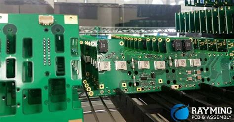
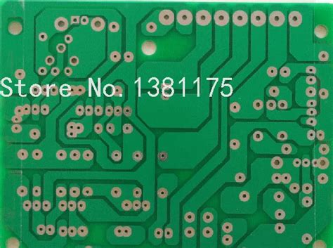
Manufacturing Techniques for High-Speed Flex PCBs
In the realm of modern electronics, the demand for high-speed flex PCBs (Printed Circuit Boards) has surged, driven by the need for compact, efficient, and reliable electronic devices. As technology advances, the manufacturing techniques for these sophisticated components have evolved to meet the stringent requirements of high-speed applications. Understanding these techniques is crucial for ensuring optimal performance and reliability in various electronic devices.
To begin with, the choice of materials plays a pivotal role in the manufacturing of high-speed flex PCBs.
The substrate material must possess excellent electrical properties, such as low dielectric constant and low loss tangent, to minimize signal loss and ensure signal integrity at high frequencies. Polyimide is a popular choice due to its flexibility, thermal stability, and excellent electrical characteristics. Additionally, the use of advanced copper foils with smooth surfaces helps reduce signal attenuation and improve overall performance.
Transitioning from materials to design considerations, the layout of high-speed flex PCBs requires meticulous attention to detail.
Signal integrity is paramount, and designers must carefully manage impedance control, crosstalk, and electromagnetic interference (EMI). Techniques such as differential signaling, controlled impedance traces, and proper grounding are employed to mitigate these issues. Moreover, the use of simulation tools during the design phase allows engineers to predict and address potential signal integrity problems before fabrication.
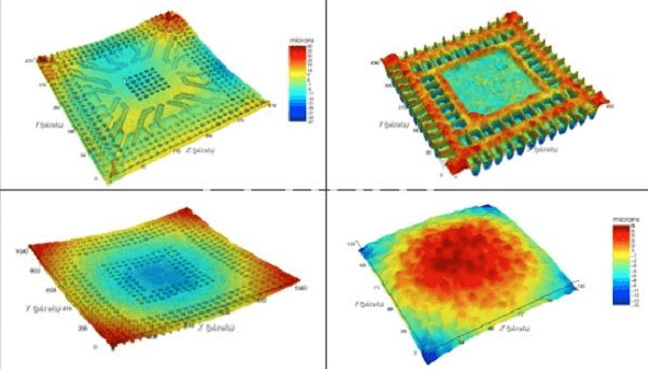
As we delve into the fabrication process, precision and accuracy are of utmost importance.
Advanced photolithography techniques are employed to create fine traces and intricate patterns on the flex PCB. This process involves coating the substrate with a photosensitive material, exposing it to a pattern of light, and then developing the image to etch away unwanted copper. The precision of this process ensures that the high-speed signals can travel with minimal distortion.
Furthermore, the lamination process is critical in the manufacturing of multilayer flex PCBs.
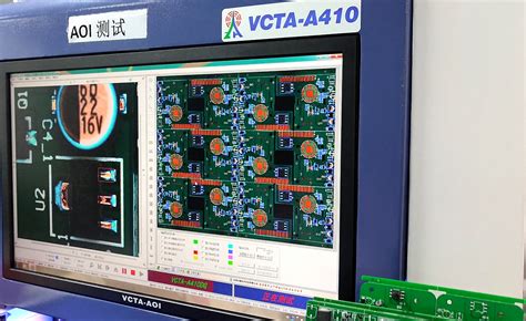
This involves bonding multiple layers of substrate and copper together under heat and pressure. The alignment of these layers must be exact to prevent misalignment, which can lead to signal degradation. The use of automated optical inspection (AOI) systems during this stage helps detect any defects or misalignments, ensuring the integrity of the final product.
In addition to these techniques, the surface finish of the flex PCB is another crucial aspect that impacts performance.
A smooth and even surface finish, such as immersion gold or ENIG (Electroless Nickel Immersion Gold), is often applied to enhance solderability and protect the copper traces from oxidation. This step is essential for maintaining the longevity and reliability of the high-speed flex PCB in various environmental conditions.
Finally, as we consider the testing and quality assurance phase, rigorous testing protocols are implemented to ensure that the high-speed flex PCBs meet the required specifications. Electrical testing, such as time-domain reflectometry (TDR) and vector network analysis, is conducted to verify signal integrity and impedance control. Additionally, mechanical testing ensures that the flex PCB can withstand bending and flexing without compromising performance.
In conclusion, the manufacturing techniques for high-speed flex PCBs are a complex interplay of material selection, design precision, fabrication accuracy, and thorough testing. As technology continues to advance, these techniques will undoubtedly evolve, paving the way for even more sophisticated and high-performing electronic devices. Understanding and mastering these techniques is essential for manufacturers aiming to produce high-speed flex PCBs that meet the ever-increasing demands of the electronics industry.