Flex pcb kicad
Introduction To Designing Flex PCBs In KiCad
Designing flexible printed circuit boards (PCBs) has become increasingly popular in the electronics industry due to their adaptability and space-saving advantages. As technology advances, the demand for compact and efficient electronic devices continues to grow, making flex PCBs an attractive solution. KiCad, an open-source electronic design automation (EDA) tool, offers a robust platform for designing these flexible circuits. Understanding the process of designing flex PCBs in KiCad is essential for engineers and designers looking to leverage the benefits of flexible electronics.
To begin with, it is important to recognize the unique characteristics of flex PCBs.
Unlike traditional rigid PCBs, flex PCBs are made from flexible materials such as polyimide, which allows them to bend and conform to various shapes. This flexibility enables the design of compact devices with complex geometries, making them ideal for applications in wearable technology, medical devices, and aerospace industries. The design process in KiCad involves several key steps, each requiring careful consideration to ensure the final product meets the desired specifications.
The first step in designing a flex PCB in KiCad is to create a schematic diagram.
This involves defining the electrical connections and components that will be used in the circuit. KiCad provides a comprehensive library of components, allowing designers to easily select and place the necessary elements onto the schematic. It is crucial to ensure that the schematic accurately represents the intended functionality of the circuit, as any errors at this stage can lead to issues in the final design.
Once the schematic is complete, the next step is to design the PCB layout.
This involves arranging the components on the board and routing the electrical connections between them. In the case of flex PCBs, special attention must be paid to the board’s mechanical properties. KiCad allows designers to define custom board shapes, which is particularly useful for flex PCBs that need to fit into non-standard enclosures. Additionally, designers must consider the bend radius and other mechanical constraints to prevent damage to the circuit during operation.
KiCad’s powerful routing tools facilitate the creation of complex trace patterns, which are essential for optimizing the performance of flex PCBs.
Designers can use these tools to minimize signal interference and ensure reliable electrical connections. Furthermore, KiCad supports the use of multiple layers, allowing for more intricate designs that can accommodate a higher density of components and connections.
After completing the layout, it is essential to perform a thorough design rule check (DRC) to identify any potential issues.
KiCad’s DRC tool helps ensure that the design adheres to the specified manufacturing constraints and industry standards. This step is crucial for preventing costly errors during the fabrication process.
Finally, once the design is verified, the next step is to generate the necessary files for manufacturing.
KiCad can produce industry-standard Gerber files, which are used by PCB manufacturers to fabricate the board. It is important to review these files carefully to ensure that they accurately represent the intended design.
In conclusion, designing flex PCBs in KiCad involves a series of well-defined steps, each requiring careful attention to detail. By leveraging KiCad’s comprehensive tools and features, designers can create flexible circuits that meet the demands of modern electronic applications. As the demand for flexible electronics continues to grow, mastering the design process in KiCad will be an invaluable skill for engineers and designers alike.
Best Practices For Flex PCB Layout In KiCad
Designing flexible printed circuit boards (PCBs) in KiCad requires a meticulous approach to ensure both functionality and durability. Flex PCBs, known for their ability to bend and conform to various shapes, are increasingly used in modern electronics due to their versatility. However, their unique properties necessitate specific design considerations to prevent mechanical and electrical failures. By adhering to best practices, designers can optimize their flex PCB layouts in KiCad, ensuring robust performance and reliability.
To begin with, understanding the material properties of flex PCBs is crucial.
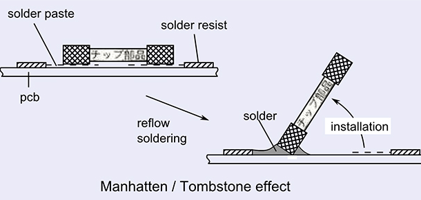
Unlike rigid PCBs, flex circuits are made from flexible substrates such as polyimide, which can withstand bending and twisting. This flexibility, while advantageous, also introduces potential stress points that can lead to circuit failure if not properly managed. Therefore, when designing in KiCad, it is essential to incorporate generous bend radii. A larger bend radius reduces stress on the copper traces, minimizing the risk of cracking or delamination. As a rule of thumb, the bend radius should be at least ten times the thickness of the flex PCB.
Transitioning to trace layout, it is important to consider the orientation and routing of traces.
In flex PCBs, traces should ideally run perpendicular to the bend lines to reduce stress. Additionally, using curved traces instead of sharp angles can further alleviate stress concentrations. KiCad offers tools to facilitate smooth trace routing, which can be leveraged to create more resilient designs. Moreover, maintaining consistent trace widths and spacing is vital to ensure uniform current distribution and prevent hot spots, which can lead to premature failure.
Another critical aspect is the stack-up configuration. Flex PCBs can be single-sided, double-sided, or multilayered, each with its own set of challenges.
In KiCad, careful planning of the layer stack-up is necessary to balance flexibility with electrical performance. For multilayer designs, it is advisable to place ground and power planes on separate layers to minimize electromagnetic interference and ensure signal integrity. Additionally, incorporating stiffeners in areas that require additional support can enhance mechanical stability without compromising flexibility.
Furthermore, the choice of vias and pads plays a significant role in the reliability of flex PCBs.
In KiCad, designers should opt for teardrop-shaped pads and vias, which provide additional mechanical support and reduce stress concentrations. This design choice is particularly beneficial in areas subject to frequent bending. Additionally, using through-hole vias instead of blind or buried vias can improve mechanical strength, although this may slightly reduce flexibility.
Thermal management is another consideration that cannot be overlooked.
Flex PCBs, due to their thin profile, can be more susceptible to thermal stress. In KiCad, designers should ensure adequate thermal relief for components and consider the use of thermal vias to dissipate heat effectively. This is especially important in high-power applications where excessive heat can lead to material degradation and failure.
Finally, thorough testing and simulation are indispensable in the design process.
KiCad provides simulation tools that allow designers to model the electrical and mechanical behavior of their flex PCB layouts. By simulating different scenarios, potential issues can be identified and addressed before fabrication, saving time and resources.
In conclusion, designing flex PCBs in KiCad requires a comprehensive understanding of both material properties and design principles. By following best practices such as optimizing bend radii, trace routing, stack-up configuration, and thermal management, designers can create reliable and efficient flex PCBs. Through careful planning and simulation, the unique challenges of flex PCB design can be effectively managed, resulting in robust and high-performing electronic solutions.

Overcoming Challenges In Flex PCB Design Using KiCad
Designing flexible printed circuit boards (PCBs) presents unique challenges that require careful consideration and specialized tools. Flex PCBs, known for their ability to bend and conform to various shapes, are increasingly used in applications where space constraints and mechanical flexibility are paramount. However, the design process for these PCBs can be complex, involving intricate layout considerations and material properties that differ significantly from traditional rigid PCBs. Fortunately, KiCad, an open-source PCB design software, offers a robust platform to address these challenges effectively.
One of the primary challenges in flex PCB design is managing the mechanical properties of the materials involved.
Unlike rigid PCBs, flex PCBs must withstand repeated bending and flexing without compromising their electrical integrity. This requires careful selection of materials and precise control over the layout to ensure durability and reliability. KiCad provides designers with the tools to simulate and visualize these mechanical stresses, allowing for the optimization of trace routing and component placement. By using KiCad’s advanced design rule checks, designers can ensure that their layouts adhere to the necessary mechanical constraints, reducing the risk of failure in the final product.
Another significant challenge in flex PCB design is the need for precise impedance control.
Flex PCBs often operate in high-frequency environments where signal integrity is critical. KiCad’s integrated simulation tools enable designers to model and analyze the electrical performance of their designs, ensuring that impedance is maintained across the board. This capability is crucial for minimizing signal loss and ensuring that the flex PCB performs as intended in its application. By leveraging KiCad’s simulation features, designers can iterate on their designs more efficiently, identifying and addressing potential issues early in the development process.
Thermal management is also a critical consideration in flex PCB design.
The thin and flexible nature of these boards can lead to challenges in dissipating heat, which can affect performance and reliability. KiCad assists designers in addressing thermal issues by providing tools for thermal analysis and management. By simulating heat distribution across the board, designers can identify hotspots and optimize their designs to improve heat dissipation. This proactive approach helps prevent overheating and extends the lifespan of the flex PCB.
Moreover, the integration of components on a flex PCB can be more complex than on a rigid board due to the need for flexibility and space constraints.
KiCad’s comprehensive library of components and footprints simplifies this process, allowing designers to easily incorporate a wide range of components into their designs. The software’s user-friendly interface and powerful layout tools enable designers to efficiently manage component placement and routing, even in the most constrained spaces.
In conclusion, while designing flex PCBs presents unique challenges, KiCad offers a comprehensive suite of tools to overcome these obstacles. By providing capabilities for mechanical simulation, impedance control, thermal management, and component integration, KiCad empowers designers to create reliable and high-performance flex PCBs. As the demand for flexible electronics continues to grow, leveraging KiCad’s features will be instrumental in meeting the evolving needs of the industry. Through its open-source nature and continuous development, KiCad remains a valuable resource for designers seeking to navigate the complexities of flex PCB design.

Advanced Techniques For Flex PCB Prototyping With KiCad
Flex PCBs, or flexible printed circuit boards, have become increasingly popular in various industries due to their ability to bend and conform to different shapes, making them ideal for compact and complex electronic devices. As the demand for these versatile circuits grows, so does the need for efficient prototyping tools. KiCad, an open-source PCB design software, offers a robust platform for designing flex PCBs, but mastering its advanced techniques can significantly enhance the prototyping process.
To begin with, understanding the unique characteristics of flex PCBs is crucial.
Unlike rigid PCBs, flex circuits are made from flexible materials such as polyimide, which allows them to bend and twist without breaking. This flexibility introduces additional design considerations, such as the need to minimize stress on the circuit traces and components. KiCad provides several features that can help address these challenges, starting with its layer management capabilities. By effectively utilizing KiCad’s layer stack-up options, designers can create a detailed representation of the flex PCB’s structure, ensuring that each layer is correctly aligned and optimized for flexibility.
Moreover, KiCad’s design rule check (DRC) feature is invaluable for flex PCB prototyping.
This tool allows designers to set specific rules that account for the unique requirements of flex circuits, such as minimum bend radius and trace width. By configuring these parameters, designers can automatically detect potential issues that could compromise the circuit’s integrity during bending. This proactive approach not only saves time but also reduces the likelihood of costly errors in the final product.
Transitioning to the layout phase, KiCad’s interactive routing tools offer significant advantages for flex PCB design.
The software’s push-and-shove router allows for precise control over trace placement, which is essential for maintaining signal integrity in flexible circuits. Additionally, KiCad supports differential pair routing, a critical feature for high-speed signal transmission. By leveraging these tools, designers can ensure that their flex PCBs meet both electrical and mechanical requirements.
Another advanced technique involves the use of KiCad’s 3D viewer, which provides a realistic visualization of the flex PCB design.
This feature is particularly beneficial for flex circuits, as it allows designers to simulate how the PCB will behave in its intended application. By examining the 3D model, designers can identify potential mechanical conflicts and make necessary adjustments before proceeding to fabrication. This step is crucial for avoiding costly iterations and ensuring that the final product meets all design specifications.
Furthermore, KiCad’s integration with external simulation tools can enhance the prototyping process.
By exporting the design to simulation software, designers can perform thermal and mechanical analyses to predict how the flex PCB will perform under various conditions. This capability is especially important for applications where the circuit will be subjected to dynamic movements or extreme temperatures.
In conclusion, mastering advanced techniques in KiCad for flex PCB prototyping can significantly improve the efficiency and accuracy of the design process. By leveraging the software’s layer management, design rule checks, interactive routing, 3D visualization, and simulation integration, designers can create high-quality flex circuits that meet the demanding requirements of modern electronic devices. As the technology continues to evolve, staying informed about the latest tools and techniques will be essential for those looking to excel in the field of flex PCB design.