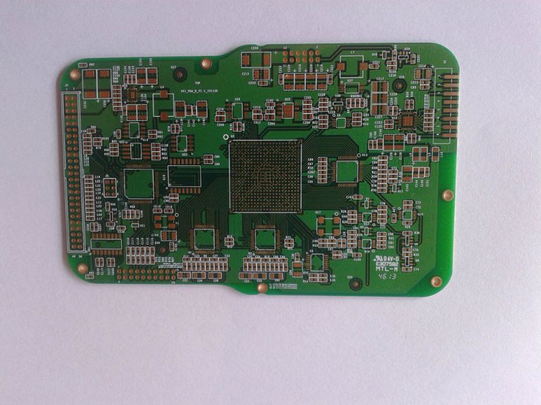
Flex pcb layers
Advantages Of Multi-Layer Flex PCBs
Multi-layer flexible printed circuit boards (PCBs) have become increasingly popular in various industries due to their numerous advantages over traditional single-layer and rigid PCBs.
One of the primary benefits of multi-layer flex PCBs is their ability to accommodate complex circuit designs.
By incorporating multiple layers, these PCBs can support intricate electrical pathways and interconnections, which are essential for advanced electronic devices. This capability allows engineers to design more sophisticated and compact products, ultimately enhancing the functionality and performance of the final application.
In addition to supporting complex designs, multi-layer flex PCBs offer significant space-saving advantages.
The flexible nature of these PCBs enables them to be bent, folded, or twisted to fit into tight spaces within electronic devices. This flexibility is particularly beneficial in applications where space is at a premium, such as in medical devices, wearable technology, and aerospace systems. By utilizing multi-layer flex PCBs, manufacturers can create smaller, lighter, and more efficient products without compromising on performance or reliability.
Another notable advantage of multi-layer flex PCBs is their improved signal integrity.
The multiple layers in these PCBs allow for better separation of signal and power planes, reducing the risk of electromagnetic interference (EMI) and crosstalk between signals. This separation is crucial for maintaining the integrity of high-speed signals and ensuring the overall performance of the electronic device. Furthermore, the ability to incorporate ground planes and shielding layers within the PCB stack-up enhances the overall electromagnetic compatibility (EMC) of the device, making it more robust and reliable in various operating environments.
Thermal management is another area where multi-layer flex PCBs excel.
The additional layers in these PCBs can be used to incorporate thermal vias and heat dissipation structures, which help to manage and dissipate heat generated by high-power components. Effective thermal management is essential for maintaining the longevity and reliability of electronic devices, particularly in applications where high temperatures are a concern. By using multi-layer flex PCBs, manufacturers can ensure that their products remain cool and operate efficiently, even under demanding conditions.
Moreover, multi-layer flex PCBs offer enhanced mechanical durability compared to their single-layer counterparts.
The multiple layers provide added strength and resilience, making these PCBs more resistant to mechanical stress and environmental factors such as vibration and shock. This increased durability is particularly important in applications where the PCB may be subjected to harsh conditions or frequent movement, such as in automotive and industrial applications. By choosing multi-layer flex PCBs, manufacturers can ensure that their products are built to withstand the rigors of real-world use.
In conclusion, the advantages of multi-layer flex PCBs are numerous and significant.
Their ability to support complex designs, save space, improve signal integrity, manage thermal performance, and enhance mechanical durability make them an ideal choice for a wide range of applications. As technology continues to advance and the demand for smaller, more efficient electronic devices grows, the adoption of multi-layer flex PCBs is likely to increase. By leveraging the benefits of these advanced PCBs, manufacturers can create innovative and high-performing products that meet the evolving needs of their customers.
Design Considerations For Single-Layer Flex PCBs
When designing single-layer flexible printed circuit boards (flex PCBs), several critical considerations must be taken into account to ensure optimal performance and reliability. The unique properties of flex PCBs, such as their ability to bend and conform to various shapes, make them ideal for applications where space constraints and mechanical flexibility are paramount. However, these same properties also introduce specific design challenges that must be addressed meticulously.
One of the primary considerations in designing single-layer flex PCBs is the selection of materials.
The substrate material, typically polyimide, must be chosen for its excellent thermal stability, mechanical strength, and flexibility. Polyimide’s ability to withstand high temperatures without deforming or losing its mechanical properties makes it an ideal choice for flex PCBs. Additionally, the copper foil used for the conductive traces must be carefully selected to balance flexibility with electrical performance. Thinner copper layers are generally preferred to enhance flexibility, but they must still provide adequate current-carrying capacity and signal integrity.
Another crucial aspect is the layout of the conductive traces.
In single-layer flex PCBs, the traces are confined to one side of the substrate, which necessitates careful planning to avoid issues such as signal crosstalk and impedance mismatches. The trace width and spacing must be optimized to ensure reliable electrical performance while maintaining the board’s flexibility. It is also essential to consider the bend radius of the flex PCB, as excessively tight bends can cause mechanical stress and potential failure of the conductive traces. Designers often use curved traces instead of sharp angles to distribute stress more evenly and enhance the board’s durability.
The placement of components on single-layer flex PCBs also requires careful consideration.
Since components are typically mounted on the same side as the conductive traces, space management becomes a critical factor. Designers must ensure that there is sufficient room for both the traces and the components, while also considering the mechanical constraints imposed by the flexing of the board. Additionally, the use of surface-mount technology (SMT) components is often preferred over through-hole components, as SMT components are generally smaller and lighter, contributing to the overall flexibility of the PCB.
Thermal management is another important consideration in the design of single-layer flex PCBs.
The thin and flexible nature of these boards can make them more susceptible to thermal stress, which can affect both the mechanical and electrical performance. Proper thermal management techniques, such as the use of thermal vias and heat sinks, must be employed to dissipate heat effectively and prevent damage to the board and its components.
Furthermore, the manufacturing process for single-layer flex PCBs must be carefully controlled to ensure high quality and reliability.
The lamination process, in particular, requires precise temperature and pressure control to avoid defects such as delamination or warping. Additionally, the etching process must be carefully monitored to ensure that the conductive traces are accurately formed without over-etching or under-etching, which can compromise the board’s performance.
In conclusion, designing single-layer flex PCBs involves a complex interplay of material selection, trace layout, component placement, thermal management, and manufacturing precision. By carefully considering these factors, designers can create flex PCBs that meet the stringent requirements of modern electronic applications, providing both mechanical flexibility and reliable electrical performance. The unique challenges posed by single-layer flex PCBs necessitate a thorough understanding of both the materials and the design principles involved, ensuring that the final product is both robust and functional.
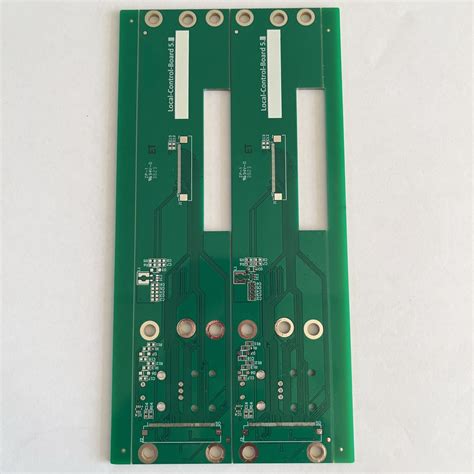
Manufacturing Process Of Double-Layer Flex PCBs
The manufacturing process of double-layer flexible printed circuit boards (PCBs) is a sophisticated and intricate procedure that demands precision and expertise. This process begins with the selection of appropriate materials, which are crucial for ensuring the flexibility and durability of the final product. Typically, polyimide is chosen for its excellent thermal stability and mechanical properties. The copper foil, which serves as the conductive layer, is laminated onto the polyimide substrate using an adhesive. This initial step sets the foundation for the subsequent stages of manufacturing.
Following the material selection and lamination, the next phase involves the creation of the circuit pattern.
This is achieved through a process known as photolithography. A photoresist, which is a light-sensitive material, is applied to the copper-clad laminate. The desired circuit pattern is then transferred onto the photoresist using ultraviolet (UV) light. The areas exposed to the UV light harden, while the unexposed areas remain soft and can be washed away using a developer solution. This leaves behind a precise pattern of the circuit on the copper layer.
Once the circuit pattern is established, the next step is etching.
During this process, the exposed copper areas are removed using a chemical etchant, typically ferric chloride or ammonium persulfate. The photoresist protects the desired circuit paths from being etched away. After the etching process is complete, the remaining photoresist is stripped away, revealing the copper circuit pattern on the polyimide substrate.
To create a double-layer flex PCB, it is necessary to establish electrical connections between the two layers.
This is accomplished through the formation of vias, which are small holes drilled through the substrate. These vias are then plated with copper to create a conductive pathway between the top and bottom layers. The drilling of vias requires high precision to ensure accurate alignment and connectivity.
Following the via formation, the next step is the application of a coverlay or solder mask.
The coverlay is a protective layer that insulates the circuit and provides mechanical protection. It is typically made of polyimide and is laminated onto the circuit using heat and pressure. The coverlay has openings that expose the pads and vias, allowing for subsequent soldering and component placement.
The final stages of the manufacturing process involve surface finishing and testing.
Surface finishing is essential for enhancing the solderability and corrosion resistance of the copper pads. Common surface finishes include immersion gold, immersion silver, and organic solderability preservatives (OSP). These finishes ensure reliable electrical connections and long-term performance of the flex PCB.
Testing is a critical step to verify the functionality and reliability of the double-layer flex PCB.
Electrical tests, such as continuity and insulation resistance tests, are conducted to ensure that the circuit paths are correctly formed and that there are no short circuits or open circuits. Additionally, mechanical tests may be performed to assess the flexibility and durability of the PCB under various conditions.
In conclusion, the manufacturing process of double-layer flex PCBs involves a series of meticulous steps, from material selection and circuit patterning to via formation, coverlay application, surface finishing, and testing. Each stage requires precision and expertise to ensure the production of high-quality, reliable, and flexible PCBs that meet the stringent demands of modern electronic applications.

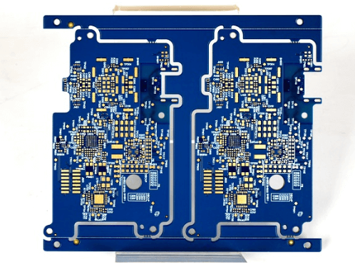
Applications Of Rigid-Flex PCBs In Modern Electronics
Rigid-flex printed circuit boards (PCBs) have become a cornerstone in the evolution of modern electronics, offering a unique combination of the durability of rigid PCBs and the flexibility of flexible circuits. This hybrid technology has opened up a myriad of applications across various industries, driven by the need for compact, reliable, and versatile electronic solutions. The integration of rigid and flexible layers within a single PCB design allows for more complex and efficient circuitry, which is particularly advantageous in today’s rapidly advancing technological landscape.
One of the most prominent applications of rigid-flex PCBs is in the consumer electronics sector.
Devices such as smartphones, tablets, and wearable technology benefit immensely from the space-saving and weight-reducing properties of rigid-flex PCBs. The ability to fold and bend the flexible sections of the PCB enables manufacturers to design thinner and more compact devices without compromising on functionality. This is particularly crucial in the development of wearable technology, where comfort and portability are paramount. The rigid sections provide the necessary structural support for components that require stability, while the flexible sections allow for movement and adaptability.
In the medical field, rigid-flex PCBs are instrumental in the development of advanced diagnostic and therapeutic devices.
Medical equipment such as pacemakers, hearing aids, and imaging devices rely on the reliability and precision of rigid-flex PCBs. The flexibility of these PCBs allows for the creation of devices that can conform to the human body’s contours, enhancing patient comfort and device efficacy. Moreover, the robust nature of rigid-flex PCBs ensures that these critical devices can withstand the demanding conditions of medical environments, including exposure to various bodily fluids and sterilization processes.
The aerospace and defense industries also leverage the advantages of rigid-flex PCBs.
In aerospace applications, the need for lightweight yet durable components is paramount. Rigid-flex PCBs meet these requirements by reducing the overall weight of electronic systems while maintaining high reliability and performance. These PCBs are used in a variety of aerospace applications, including avionics, satellite systems, and unmanned aerial vehicles (UAVs). In defense, the ruggedness and flexibility of rigid-flex PCBs make them ideal for use in military communication systems, radar systems, and other mission-critical equipment. The ability to withstand extreme temperatures, vibrations, and other harsh conditions ensures that these systems remain operational in the most challenging environments.
Automotive electronics is another domain where rigid-flex PCBs have made significant inroads.
Modern vehicles are equipped with a plethora of electronic systems, from advanced driver-assistance systems (ADAS) to infotainment and navigation systems. Rigid-flex PCBs enable the integration of these complex systems within the limited space available in vehicles. The flexibility of the PCBs allows for innovative design solutions, such as routing circuits through tight spaces and around obstacles, which is essential for optimizing the layout and functionality of automotive electronics.
In conclusion, the applications of rigid-flex PCBs in modern electronics are vast and varied, spanning consumer electronics, medical devices, aerospace, defense, and automotive industries. The unique combination of rigidity and flexibility offered by these PCBs provides unparalleled advantages in terms of space-saving, reliability, and design versatility. As technology continues to advance, the role of rigid-flex PCBs in enabling the development of more sophisticated and efficient electronic systems will undoubtedly expand, driving innovation across multiple sectors.