Flex pcb layout guidelines
The Flex PCB layout guidelines Design
In the realm of modern electronics, the demand for compact, lightweight, and flexible devices has led to the increasing popularity of flexible printed circuit boards (PCBs). These innovative circuits offer a myriad of advantages over their rigid counterparts, including enhanced flexibility, reduced weight, and the ability to conform to complex shapes. However, designing a flex PCB requires a nuanced understanding of specific guidelines to ensure optimal performance and reliability. As we delve into the basics of flex PCB design, it is essential to consider several critical factors that influence the overall functionality and durability of the final product.
To begin with, material selection plays a pivotal role in flex PCB design.
Unlike rigid PCBs, which typically use FR-4 as a substrate, flex PCBs often employ polyimide due to its excellent thermal stability and flexibility. This material choice not only allows the circuit to bend and twist without damage but also provides a robust foundation for the copper traces. Furthermore, the thickness of the polyimide layer must be carefully considered, as it directly impacts the board’s flexibility and mechanical strength. A balance must be struck to ensure that the board can withstand repeated flexing without compromising its structural integrity.
Transitioning to the layout of the copper traces, it is crucial to adhere to specific design principles to prevent mechanical stress and potential failure.
One such guideline is to avoid sharp corners in trace routing, as these can act as stress concentrators and lead to cracking. Instead, designers should opt for smooth, curved traces that distribute stress more evenly. Additionally, maintaining a consistent trace width and spacing is vital to ensure uniform current distribution and minimize the risk of hot spots, which can cause localized heating and damage.
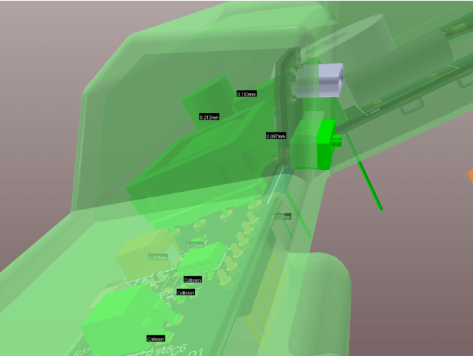
Another important consideration in flex PCB design is the implementation of appropriate bend radius guidelines.
The bend radius is the minimum radius that the board can be bent without causing damage to the copper traces or the substrate. Adhering to the recommended bend radius is essential to prevent mechanical failure and ensure the longevity of the circuit. Typically, a larger bend radius is preferred, as it reduces the stress on the materials and enhances the board’s durability. Designers must also account for dynamic flexing applications, where the board is subjected to repeated bending, by incorporating additional design features such as strain reliefs and reinforced areas.
Moreover, the use of coverlays and stiffeners is a common practice in flex PCB design to protect the copper traces and provide additional mechanical support.
Coverlays, typically made of polyimide, are applied over the copper traces to shield them from environmental factors such as moisture and dust. Stiffeners, on the other hand, are rigid materials added to specific areas of the board to provide support and facilitate component mounting. The strategic placement of these elements is crucial to maintaining the board’s flexibility while ensuring adequate protection and support.
In conclusion, designing a flex PCB involves a careful balance of material selection, trace layout, bend radius considerations, and protective measures. By adhering to these fundamental guidelines, designers can create flexible circuits that not only meet the demands of modern electronic applications but also exhibit exceptional reliability and performance. As the electronics industry continues to evolve, the importance of mastering flex PCB design principles will undoubtedly grow, paving the way for more innovative and versatile electronic devices.
Key Considerations For Flex PCB Layout
When designing a flexible printed circuit board (PCB), several key considerations must be taken into account to ensure optimal performance and reliability. Flex PCBs, known for their ability to bend and conform to various shapes, are increasingly used in applications where space constraints and mechanical flexibility are paramount. As such, understanding the unique requirements of flex PCB layout is crucial for engineers and designers.
To begin with, material selection plays a pivotal role in the design of flex PCBs.
Unlike rigid PCBs, flex circuits are typically made from polyimide, a material known for its excellent thermal stability and flexibility. This choice of material not only allows the circuit to bend without breaking but also provides a robust platform for the copper traces. However, the designer must carefully consider the thickness of the polyimide and copper layers, as these will directly impact the board’s flexibility and durability. Thinner materials offer greater flexibility but may be more susceptible to mechanical damage, while thicker materials provide strength at the cost of reduced flexibility.
Transitioning from material considerations, the layout of the traces on a flex PCB is another critical aspect.
Trace routing should be done with an emphasis on minimizing stress. This can be achieved by using curved traces instead of sharp angles, which can act as stress concentrators and lead to potential failure points. Additionally, traces should be routed perpendicular to the bend lines whenever possible, as this orientation reduces the likelihood of trace cracking during flexing. It is also advisable to maintain uniform trace widths and spacing to ensure even distribution of mechanical stress across the board.
Furthermore, the placement of components on a flex PCB requires careful thought.
Components should be positioned in areas that experience minimal bending to avoid mechanical stress on solder joints. In cases where components must be placed in bend areas, it is essential to use flexible adhesive or encapsulant to provide additional support. Moreover, designers should consider the use of stiffeners, which are rigid sections added to specific areas of the flex PCB to provide mechanical support and facilitate component mounting.
In addition to these considerations, the choice of coverlay material is vital for protecting the flex PCB.
Coverlay, typically made from polyimide, serves as a protective layer over the copper traces, shielding them from environmental factors such as moisture and dust. The coverlay must be carefully applied to ensure it does not impede the board’s flexibility. Designers should also ensure that the coverlay openings are accurately aligned with the pads to facilitate proper soldering during assembly.
Finally, testing and validation are indispensable steps in the flex PCB design process.
Prototyping and rigorous testing under real-world conditions help identify potential issues related to mechanical stress and electrical performance. By simulating the flexing and bending that the PCB will undergo in its intended application, designers can make necessary adjustments to enhance reliability.
In conclusion, designing a flex PCB requires a comprehensive understanding of material properties, trace routing, component placement, and protective measures. By adhering to these guidelines, engineers can create flexible circuits that meet the demands of modern electronic applications, ensuring both functionality and longevity. As technology continues to evolve, the importance of meticulous flex PCB design will only grow, underscoring the need for ongoing innovation and attention to detail in this specialized field.
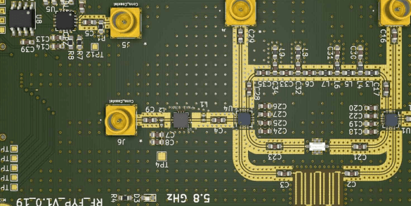
Best Practices For Flex PCB Trace Routing
In the realm of modern electronics, the demand for compact, lightweight, and flexible devices has led to the increased adoption of flexible printed circuit boards (PCBs). These innovative circuits offer a unique advantage over their rigid counterparts by allowing for dynamic bending and folding, which is essential in applications such as wearable technology, medical devices, and aerospace systems. However, designing a flex PCB requires careful consideration of trace routing to ensure reliability and performance. Adhering to best practices in flex PCB trace routing is crucial for optimizing the functionality and longevity of the circuit.
To begin with, understanding the mechanical properties of the flex PCB material is essential.
Unlike rigid PCBs, flex circuits are subject to mechanical stress due to bending and flexing. Therefore, it is imperative to design trace routing that minimizes stress concentration. One effective strategy is to use curved traces instead of sharp angles. Sharp corners can act as stress concentrators, leading to potential cracking or delamination over time. By employing smooth, gradual curves, the stress is distributed more evenly across the trace, enhancing the durability of the circuit.
Moreover, maintaining a consistent trace width is vital in flex PCB design.
Variations in trace width can lead to impedance mismatches, which may affect signal integrity. Consistent trace width ensures uniform current distribution, reducing the risk of hotspots that could lead to thermal issues. Additionally, it is advisable to use wider traces in areas subject to frequent bending. Wider traces provide greater mechanical strength and are less prone to fatigue failure.
Transitioning to the topic of trace routing layers, it is beneficial to utilize a staggered or offset arrangement for traces on different layers.
This approach minimizes the risk of stress concentration at any single point, as the traces are not directly aligned with each other. Furthermore, when designing multi-layer flex PCBs, it is crucial to consider the stack-up configuration. A balanced stack-up, where the copper layers are symmetrically distributed, helps maintain the mechanical stability of the flex circuit.
Another important aspect of flex PCB trace routing is the use of teardrop pads.
Teardrop pads are employed at the junctions where traces meet pads or vias. These pads provide a gradual transition between the trace and the pad, reducing the risk of stress concentration and potential cracking. By incorporating teardrop pads, designers can enhance the mechanical robustness of the flex PCB.
In addition to mechanical considerations, electrical performance must also be taken into account.
To minimize electromagnetic interference (EMI), it is advisable to route high-speed signals on the inner layers of the flex PCB. This approach provides shielding from external noise sources and helps maintain signal integrity. Furthermore, maintaining adequate spacing between traces is essential to prevent crosstalk, which can degrade signal quality.
Finally, it is important to consider the environmental conditions in which the flex PCB will operate.
Factors such as temperature, humidity, and exposure to chemicals can impact the performance and reliability of the circuit. Selecting appropriate materials and finishes that can withstand these conditions is crucial for ensuring the longevity of the flex PCB.
In conclusion, designing a flex PCB with optimal trace routing requires a comprehensive understanding of both mechanical and electrical considerations. By adhering to best practices such as using curved traces, maintaining consistent trace width, employing teardrop pads, and considering environmental factors, designers can create robust and reliable flex circuits that meet the demands of modern electronic applications.
Material Selection And Stackup Design In Flex PCBs
In the realm of modern electronics, the demand for flexible printed circuit boards (PCBs) has surged, driven by the need for compact, lightweight, and versatile designs. A critical aspect of designing flex PCBs is the careful selection of materials and the strategic planning of the stackup. These elements are pivotal in ensuring the functionality, reliability, and longevity of the final product. To begin with, material selection is a fundamental step in the design of flex PCBs. The choice of materials directly impacts the board’s flexibility, thermal performance, and overall durability. Polyimide is a popular substrate material due to its excellent thermal stability, mechanical strength, and flexibility. It can withstand high temperatures, making it suitable for applications that require soldering or exposure to harsh environments. Additionally, polyimide’s low dielectric constant and loss tangent contribute to superior electrical performance, which is crucial for high-frequency applications.
Moreover, the copper used in flex PCBs must be carefully considered.
Rolled annealed (RA) copper is often preferred over electro-deposited (ED) copper due to its superior ductility and fatigue resistance. RA copper’s grain structure allows it to bend and flex without cracking, which is essential for applications involving repeated flexing or dynamic movement. However, the choice between RA and ED copper may also depend on cost considerations and specific application requirements. Transitioning to the stackup design, it is essential to balance flexibility with mechanical support. A typical flex PCB stackup consists of multiple layers, including the base substrate, adhesive layers, copper layers, and coverlay. The base substrate provides the foundational support, while the adhesive layers bond the copper to the substrate. The coverlay, often made of polyimide, protects the copper traces from environmental damage and mechanical stress.
In designing the stackup, one must consider the number of layers and their arrangement.
A single-layer flex PCB is the simplest form, offering maximum flexibility but limited routing options. In contrast, multi-layer flex PCBs provide increased routing density and design complexity but may reduce flexibility. Therefore, designers must carefully evaluate the application’s requirements to determine the optimal number of layers. Furthermore, the thickness of each layer plays a crucial role in the overall flexibility and performance of the PCB. Thinner layers enhance flexibility but may compromise mechanical strength and signal integrity. Conversely, thicker layers provide robustness but at the cost of reduced flexibility. Thus, achieving the right balance is key to a successful design.
Another important consideration in stackup design is the use of stiffeners.
Stiffeners are rigid materials, such as FR-4 or stainless steel, added to specific areas of the flex PCB to provide mechanical support and facilitate component mounting. They are particularly useful in areas where connectors or other heavy components are placed, preventing excessive bending and potential damage. However, the use of stiffeners should be judicious, as they can limit the board’s flexibility. In conclusion, the material selection and stackup design in flex PCBs are critical components that require careful consideration and planning. By understanding the properties and trade-offs of different materials and stackup configurations, designers can create flex PCBs that meet the specific demands of their applications, ensuring optimal performance and reliability.