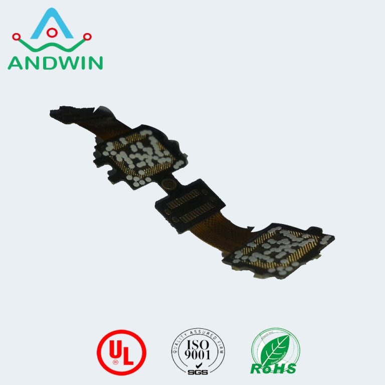
Flex pcb panelization
Benefits Of Flex PCB Panelization In Modern Electronics
Flex PCB panelization has emerged as a pivotal technique in the realm of modern electronics, offering a multitude of benefits that enhance both the manufacturing process and the performance of electronic devices. As the demand for more compact, efficient, and versatile electronic products continues to rise, the role of flex PCB panelization becomes increasingly significant. This process involves grouping multiple flexible printed circuit boards (PCBs) onto a single panel, which is then processed as a unit. By doing so, manufacturers can achieve greater efficiency and cost-effectiveness, which are crucial in today’s competitive market.
One of the primary advantages of flex PCB panelization is the optimization of manufacturing efficiency.
By processing multiple circuits simultaneously, manufacturers can significantly reduce the time and labor required for production. This not only accelerates the manufacturing timeline but also minimizes the potential for errors, as handling a single panel is inherently less complex than managing individual circuits. Consequently, this leads to a reduction in production costs, which can be particularly beneficial for large-scale operations where even minor savings per unit can accumulate to substantial financial benefits.
Moreover, flex PCB panelization contributes to material savings.
The process allows for the efficient use of substrate materials, as the layout can be optimized to minimize waste. This is particularly important in the context of flexible PCBs, where the materials used can be more expensive than those in traditional rigid PCBs. By reducing material waste, manufacturers can further lower production costs and contribute to more sustainable manufacturing practices, aligning with the growing emphasis on environmental responsibility in the electronics industry.
In addition to manufacturing benefits, flex PCB panelization also enhances the performance and reliability of electronic devices.
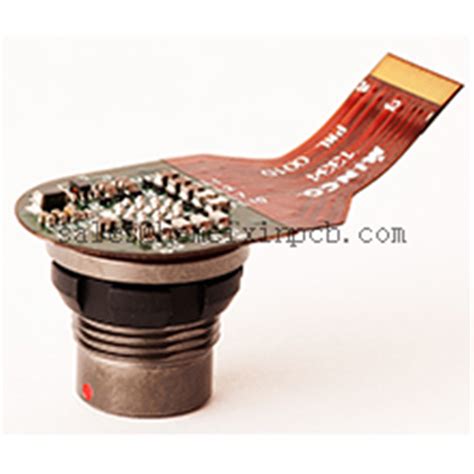
The flexibility of these circuits allows for more innovative and compact designs, which are essential in the development of modern electronics such as wearable devices, smartphones, and medical equipment. The ability to bend and fold without compromising functionality enables designers to create products that are not only smaller but also more ergonomic and user-friendly. Furthermore, the reduced number of interconnections in a panelized design can lead to improved signal integrity and reduced risk of failure, as there are fewer points of potential disconnection or malfunction.
Transitioning from the technical advantages, it is also important to consider the economic implications of flex PCB panelization.
As the electronics market becomes increasingly globalized, manufacturers are under pressure to deliver high-quality products at competitive prices. Flex PCB panelization provides a strategic advantage by enabling cost-effective production without sacrificing quality. This is particularly relevant for companies looking to expand their market share or enter new markets, as the ability to offer reliable products at lower prices can be a decisive factor in gaining a competitive edge.
In conclusion, the benefits of flex PCB panelization in modern electronics are manifold, encompassing improvements in manufacturing efficiency, material savings, device performance, and economic competitiveness. As technology continues to evolve and consumer expectations rise, the importance of innovative manufacturing techniques like flex PCB panelization will only grow. By embracing these advancements, manufacturers can not only meet current demands but also position themselves for future success in an ever-changing industry landscape.
Techniques For Efficient Flex PCB Panelization
Flex PCB panelization is a crucial process in the manufacturing of flexible printed circuit boards, aimed at optimizing production efficiency and reducing costs. This technique involves grouping multiple circuit boards onto a single panel, allowing them to be processed simultaneously. As the demand for compact and versatile electronic devices continues to grow, the importance of efficient panelization techniques cannot be overstated. By understanding and implementing effective strategies, manufacturers can significantly enhance their production capabilities while maintaining high-quality standards.
One of the primary considerations in flex PCB panelization is the layout design.
A well-thought-out design ensures that the maximum number of boards can be placed on a single panel without compromising the integrity of each individual circuit. This involves careful planning of the board’s shape, size, and orientation. By optimizing these parameters, manufacturers can minimize material waste and reduce the overall cost of production. Additionally, a strategic layout can facilitate easier handling and processing during subsequent manufacturing stages, such as soldering and assembly.
Transitioning from design to material selection, the choice of substrate plays a pivotal role in the panelization process.
Flexible PCBs are typically made from materials like polyimide or polyester, which offer excellent flexibility and thermal stability. However, the specific material chosen can impact the panelization strategy. For instance, polyimide is known for its superior heat resistance, making it suitable for applications requiring high-temperature processing. On the other hand, polyester is more cost-effective and can be used in less demanding environments. Selecting the appropriate material not only affects the performance of the final product but also influences the efficiency of the panelization process.
Furthermore, the method of separating individual boards from the panel is another critical aspect of flex PCB panelization.
Techniques such as routing, laser cutting, and punching are commonly employed to achieve this. Each method has its advantages and limitations, and the choice largely depends on the specific requirements of the project. For example, laser cutting offers high precision and is ideal for intricate designs, but it may be more expensive compared to other methods. Conversely, punching is a cost-effective solution for simpler designs but may not provide the same level of accuracy. By carefully selecting the appropriate separation technique, manufacturers can ensure that the boards are detached cleanly and efficiently, minimizing the risk of damage.
In addition to these technical considerations, manufacturers must also account for the economic aspects of flex PCB panelization.
The cost of materials, labor, and equipment all contribute to the overall expense of the process. By optimizing panelization techniques, manufacturers can achieve economies of scale, reducing the cost per unit and enhancing profitability. This involves not only maximizing the number of boards per panel but also streamlining the entire production process to minimize downtime and waste.
In conclusion, efficient flex PCB panelization is a multifaceted process that requires careful consideration of design, material selection, separation techniques, and economic factors. By employing strategic approaches in each of these areas, manufacturers can enhance their production efficiency, reduce costs, and deliver high-quality products to meet the growing demands of the electronics industry. As technology continues to evolve, the importance of mastering these techniques will only become more pronounced, underscoring the need for ongoing innovation and adaptation in the field of flex PCB manufacturing.
Challenges And Solutions In Flex PCB Panelization
Flex PCB panelization, a critical process in the manufacturing of flexible printed circuit boards, presents a unique set of challenges and solutions that are essential for ensuring efficiency and quality in production. As the demand for smaller, lighter, and more versatile electronic devices continues to grow, the need for flexible PCBs has become increasingly prominent. However, the panelization of these flexible circuits is not without its complexities.
One of the primary challenges in flex PCB panelization is the inherent flexibility of the material itself.
Unlike rigid PCBs, flexible circuits can bend and twist, which can lead to difficulties in maintaining alignment during the manufacturing process. This flexibility, while advantageous in the final application, requires careful handling and precise engineering to ensure that the circuits remain intact and functional. To address this, manufacturers often employ specialized fixtures and support materials during the panelization process to maintain the necessary rigidity and alignment.
Moreover, the thinness of flex PCBs poses another significant challenge.
The reduced thickness, while beneficial for applications requiring minimal space, can lead to issues such as warping and tearing during the panelization and subsequent manufacturing stages. To mitigate these risks, manufacturers may use reinforcement layers or incorporate stiffeners in specific areas of the PCB. These solutions help to provide additional support and prevent damage, ensuring that the flex PCBs can withstand the rigors of production and assembly.
In addition to physical challenges, flex PCB panelization also involves intricate design considerations.
The layout of the circuits must be meticulously planned to optimize space and functionality while minimizing waste. This often requires advanced software tools that can simulate the panelization process and identify potential issues before they arise. By utilizing these tools, designers can create more efficient layouts that reduce material costs and improve yield rates.
Furthermore, the choice of materials plays a crucial role in the success of flex PCB panelization.
The materials used must not only be flexible but also durable enough to withstand the environmental conditions they will encounter in their final application. This includes resistance to heat, moisture, and mechanical stress. Manufacturers must carefully select materials that balance these requirements while also being cost-effective. Advances in material science have led to the development of new substrates and adhesives that enhance the performance and reliability of flex PCBs, providing manufacturers with more options to address these challenges.
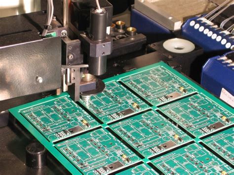
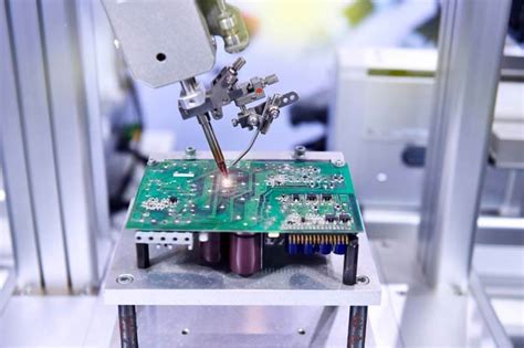
Another solution to the challenges of flex PCB panelization is the implementation of automated processes.
Automation can significantly improve the precision and consistency of the panelization process, reducing the likelihood of human error and increasing production efficiency. Automated systems can handle the delicate nature of flex PCBs with greater accuracy, ensuring that each panel is produced to the exact specifications required.
In conclusion, while flex PCB panelization presents several challenges, there are numerous solutions available to address these issues. By employing specialized fixtures, advanced design software, careful material selection, and automation, manufacturers can overcome the difficulties associated with the flexibility and thinness of these circuits. As technology continues to advance, it is likely that new innovations will further enhance the panelization process, making it even more efficient and reliable. This will undoubtedly contribute to the continued growth and success of the flexible electronics industry, meeting the ever-increasing demand for innovative and adaptable electronic solutions.
Innovations In Flex PCB Panelization Technology
Flex PCB panelization technology has undergone significant advancements in recent years, driven by the increasing demand for more compact, efficient, and versatile electronic devices. As the electronics industry continues to evolve, the need for flexible printed circuit boards (PCBs) that can accommodate complex designs and fit into unconventional spaces has become more pronounced. Consequently, innovations in flex PCB panelization have emerged as a critical area of focus, offering solutions that enhance manufacturing efficiency, reduce costs, and improve the overall performance of electronic products.
One of the most notable innovations in flex PCB panelization is the development of advanced materials that offer superior flexibility and durability.
These materials, often composed of polyimide or polyester films, provide excellent thermal stability and resistance to environmental stressors, making them ideal for use in a wide range of applications. By utilizing these advanced materials, manufacturers can produce flex PCBs that maintain their integrity even under extreme conditions, thereby extending the lifespan of the electronic devices in which they are used.
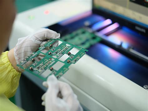
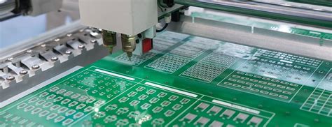
In addition to material advancements, the introduction of automated panelization processes has revolutionized the way flex PCBs are manufactured.
Automation technologies, such as computer-aided design (CAD) software and robotic assembly systems, have streamlined the panelization process, allowing for greater precision and consistency in the production of flex PCBs. These technologies enable manufacturers to optimize the layout of multiple circuit boards on a single panel, minimizing waste and maximizing the use of available space. As a result, the production of flex PCBs has become more cost-effective and efficient, meeting the growing demand for high-quality electronic components.
Moreover, innovations in flex PCB panelization have also focused on improving the scalability of production processes.
With the rise of the Internet of Things (IoT) and wearable technology, there is an increasing need for small-scale, flexible electronic components that can be produced in large quantities. To address this demand, manufacturers have developed scalable panelization techniques that allow for the mass production of flex PCBs without compromising on quality or performance. These techniques often involve the use of modular panel designs, which can be easily adjusted to accommodate different circuit configurations and sizes, thereby enhancing the versatility of flex PCB manufacturing.
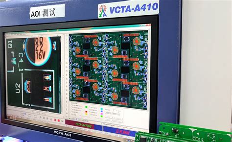
Furthermore, the integration of advanced inspection and testing technologies has played a crucial role in ensuring the reliability and functionality of flex PCBs.
Automated optical inspection (AOI) systems and X-ray inspection technologies have become integral components of the panelization process, enabling manufacturers to detect and rectify defects at an early stage. By incorporating these inspection methods, manufacturers can ensure that each flex PCB meets stringent quality standards, reducing the likelihood of failures and enhancing the overall performance of electronic devices.
In conclusion, the innovations in flex PCB panelization technology have significantly transformed the electronics manufacturing landscape.
Through advancements in materials, automation, scalability, and inspection technologies, manufacturers are now able to produce high-quality, reliable, and cost-effective flex PCBs that meet the diverse needs of modern electronic devices. As the demand for flexible electronic components continues to grow, it is expected that further innovations in flex PCB panelization will continue to emerge, driving the industry towards even greater levels of efficiency and performance.