Flex pcb rules
Design Guidelines for Flex PCB Layout
In the realm of modern electronics, flexible printed circuit boards (flex PCBs) have emerged as a pivotal component, offering unparalleled versatility and adaptability. As the demand for compact and efficient electronic devices continues to rise, understanding the design guidelines for flex PCB layout becomes increasingly crucial. These guidelines not only ensure optimal performance but also enhance the durability and reliability of the final product.
To begin with, one must consider the unique properties of flex PCBs, which distinguish them from their rigid counterparts.
Flex PCBs are designed to bend and twist, allowing them to fit into spaces that rigid boards cannot. This flexibility necessitates a careful approach to layout design, as improper handling can lead to mechanical failures. Therefore, it is essential to incorporate bend radius considerations into the design process. The bend radius is the minimum radius one can bend the flex PCB without causing damage. A general rule of thumb is to maintain a bend radius of at least ten times the thickness of the flex material. This precaution helps prevent stress fractures and ensures the longevity of the circuit.
Moreover, trace routing plays a significant role in the design of flex PCBs.
Unlike rigid boards, where traces can be laid out in straight lines without much concern, flex PCBs require a more strategic approach. It is advisable to use curved traces instead of sharp angles, as this reduces stress concentration and enhances the board’s flexibility. Additionally, staggering traces on different layers can help distribute mechanical stress more evenly, further contributing to the board’s durability.
Transitioning to the topic of material selection, it is imperative to choose materials that complement the flex PCB’s intended application.
Polyimide is a popular choice due to its excellent thermal stability and flexibility. However, the choice of adhesive and coverlay materials also plays a critical role in the board’s performance. These materials should be selected based on their ability to withstand the environmental conditions the PCB will encounter, such as temperature fluctuations and exposure to chemicals.
Furthermore, the importance of proper via design cannot be overstated.
Vias are used to connect different layers of a PCB, and in flex designs, they must be carefully planned to avoid compromising the board’s flexibility. It is recommended to use teardrop-shaped pads for vias, as this design reduces stress concentration around the via and minimizes the risk of cracking. Additionally, keeping vias away from bend areas can prevent mechanical failures during flexing.
In addition to these technical considerations, it is also vital to account for manufacturing tolerances.
Flex PCBs are subject to variations during the manufacturing process, and designers must accommodate these tolerances to ensure the final product meets specifications. This includes allowing for potential shrinkage or expansion of materials and ensuring that all components are placed with sufficient clearance to avoid interference.
In conclusion, designing a flex PCB layout requires a comprehensive understanding of the unique challenges and opportunities presented by flexible circuits. By adhering to these guidelines—considering bend radius, optimizing trace routing, selecting appropriate materials, designing robust vias, and accounting for manufacturing tolerances—designers can create flex PCBs that are not only functional but also reliable and durable. As technology continues to evolve, the role of flex PCBs will undoubtedly expand, making these design principles all the more essential for future innovations.
Material Selection for Flexible PCBs
When designing flexible printed circuit boards (PCBs), the selection of materials plays a crucial role in determining the performance, reliability, and cost-effectiveness of the final product. Flexible PCBs, known for their ability to bend and conform to various shapes, are increasingly used in applications where space constraints and mechanical flexibility are paramount. Therefore, understanding the properties and implications of different materials is essential for engineers and designers aiming to optimize their designs.
To begin with, the substrate material is a fundamental consideration in flexible PCB design.
Polyimide is the most commonly used substrate due to its excellent thermal stability, mechanical strength, and flexibility. It can withstand high temperatures, making it suitable for applications that require soldering or exposure to harsh environments. Additionally, polyimide’s low dielectric constant and loss tangent contribute to superior electrical performance, which is critical in high-frequency applications. However, it is important to note that polyimide can be relatively expensive compared to other materials, which may impact the overall cost of the PCB.
In contrast, polyester is another substrate option that offers a more cost-effective solution.
While it does not possess the same high-temperature resistance as polyimide, polyester is suitable for applications with lower thermal demands. Its flexibility and ease of processing make it an attractive choice for consumer electronics and other cost-sensitive applications. However, designers must carefully evaluate the trade-offs between cost and performance when opting for polyester substrates.
Moving on to the conductive materials, copper is the standard choice for flexible PCBs due to its excellent electrical conductivity and ductility.
Copper can be deposited onto the substrate using various methods, such as electroplating or laminating copper foil. The thickness of the copper layer is a critical factor that influences the current-carrying capacity and flexibility of the PCB. Thinner copper layers enhance flexibility but may limit the current capacity, whereas thicker layers provide better current handling but reduce flexibility. Therefore, selecting the appropriate copper thickness requires a careful balance between electrical and mechanical requirements.
Furthermore, the choice of adhesive materials is another vital aspect of flexible PCB design.
Adhesives are used to bond the copper layers to the substrate and to laminate multiple layers together in multilayer designs. Acrylic and epoxy adhesives are commonly used, each offering distinct advantages. Acrylic adhesives provide excellent flexibility and are well-suited for dynamic flex applications where repeated bending occurs. On the other hand, epoxy adhesives offer superior thermal and chemical resistance, making them ideal for applications exposed to harsh environments. The selection of adhesive materials should align with the specific application requirements and environmental conditions.
In addition to these primary materials, protective coatings such as solder masks and coverlays are essential for safeguarding the flexible PCB from environmental factors and mechanical damage. Solder masks, typically made from liquid photoimageable materials, protect the copper traces from oxidation and prevent solder bridging during assembly. Coverlays, often made from polyimide films, provide additional mechanical protection and insulation. The choice between solder masks and coverlays depends on the specific design and application needs.
In conclusion, material selection for flexible PCBs is a multifaceted process that requires careful consideration of various factors, including thermal performance, electrical conductivity, mechanical flexibility, and cost. By understanding the properties and trade-offs of different materials, designers can make informed decisions that optimize the performance and reliability of their flexible PCB designs. As technology continues to advance, ongoing research and development in materials science will likely yield new options and innovations, further enhancing the capabilities of flexible PCBs in diverse applications.
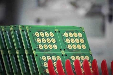
Best Practices for Flex PCB Manufacturing
In the realm of modern electronics, flexible printed circuit boards (PCBs) have emerged as a pivotal component, offering unparalleled versatility and adaptability. As the demand for compact and efficient electronic devices continues to rise, the importance of adhering to best practices in flex PCB manufacturing cannot be overstated. These best practices not only ensure the reliability and performance of the final product but also optimize the manufacturing process, reducing costs and minimizing errors.
To begin with, understanding the unique properties of flexible PCBs is crucial.
Unlike their rigid counterparts, flex PCBs are designed to bend and twist, allowing them to fit into compact spaces and conform to various shapes. This flexibility, however, introduces a set of challenges that must be addressed during the design and manufacturing stages. One of the primary considerations is the choice of materials. Selecting the appropriate substrate material, such as polyimide, is essential due to its excellent thermal stability and flexibility. Additionally, the choice of adhesive and copper foil must be carefully evaluated to ensure compatibility and durability.
Transitioning from material selection to design considerations, it is imperative to incorporate specific design rules tailored for flex PCBs.
For instance, trace routing should be meticulously planned to avoid sharp bends, which can lead to stress concentration and potential failure. Instead, gradual curves and staggered vias are recommended to distribute mechanical stress evenly. Furthermore, maintaining a consistent trace width and spacing is vital to prevent impedance mismatches and signal integrity issues. By adhering to these design principles, manufacturers can enhance the reliability and longevity of flex PCBs.
Moving forward, the manufacturing process itself demands a high level of precision and control.
One of the key steps is the etching process, where maintaining uniformity is critical to achieving the desired circuit patterns. Employing advanced etching techniques and equipment can significantly improve the accuracy and consistency of the final product. Moreover, the lamination process, which involves bonding multiple layers of the PCB, requires careful temperature and pressure control to prevent delamination and ensure structural integrity.
In addition to these technical aspects, quality control plays a pivotal role in flex PCB manufacturing.
Implementing rigorous testing protocols at various stages of production can help identify defects early, reducing the likelihood of costly rework or product failures. Techniques such as automated optical inspection (AOI) and X-ray inspection are invaluable tools for detecting issues such as misalignments, voids, and other anomalies. By integrating these quality control measures, manufacturers can uphold high standards and deliver reliable products to their clients.
Finally, it is essential to consider the environmental impact of flex PCB manufacturing.
As sustainability becomes an increasingly important factor in the electronics industry, adopting eco-friendly practices is not only beneficial for the environment but also enhances the reputation of manufacturers. Utilizing lead-free solder, recycling waste materials, and optimizing energy consumption are just a few ways to minimize the ecological footprint of the manufacturing process.
In conclusion, the successful manufacturing of flex PCBs hinges on a comprehensive understanding of material properties, meticulous design considerations, precise manufacturing techniques, and stringent quality control measures. By adhering to these best practices, manufacturers can produce high-quality, reliable flex PCBs that meet the ever-evolving demands of the electronics industry. As technology continues to advance, staying abreast of the latest developments and continuously refining manufacturing processes will be key to maintaining a competitive edge in this dynamic field.
Common Mistakes to Avoid in Flex PCB Design
In the realm of electronics, the design of flexible printed circuit boards (PCBs) is a critical task that demands precision and expertise. Flex PCBs offer numerous advantages, such as space-saving capabilities and enhanced durability, making them indispensable in modern electronic devices. However, the design process is fraught with potential pitfalls that can compromise the functionality and reliability of the final product. Understanding and avoiding these common mistakes is essential for engineers and designers aiming to create efficient and effective flex PCBs.
One prevalent mistake in flex PCB design is the improper management of bend areas.
Flex PCBs are often used in applications where bending and flexing are required, such as in wearable devices or foldable gadgets. Designers must ensure that the bend areas are free from components and vias, as these can lead to mechanical stress and eventual failure. To mitigate this risk, it is crucial to define the bend areas clearly and use appropriate materials that can withstand repeated flexing without degrading.
Another common error is neglecting to consider the thermal management of the flex PCB
Due to their compact nature, flex PCBs can be prone to overheating, which can adversely affect performance and longevity. Designers should incorporate adequate thermal management strategies, such as using thermal vias or heat sinks, to dissipate heat effectively. Additionally, selecting materials with suitable thermal properties can help in maintaining optimal operating temperatures.
Furthermore, inadequate attention to trace routing can lead to significant issues in flex PCB design.
Traces that are too narrow or improperly routed can result in increased resistance and potential signal integrity problems. It is essential to follow industry guidelines for trace width and spacing, taking into account the current-carrying capacity and the potential for electromagnetic interference. Employing simulation tools during the design phase can help identify and rectify routing issues before they become problematic.
Transitioning to another critical aspect, the choice of materials plays a pivotal role in the success of a flex PCB design.
Selecting inappropriate materials can lead to issues such as delamination or cracking, especially in applications involving frequent bending. Designers should opt for materials that offer a balance between flexibility and durability, ensuring that the PCB can withstand the mechanical stresses it will encounter in its intended application. Consulting with material suppliers and conducting thorough testing can aid in making informed material choices.
Moreover, overlooking the importance of proper documentation and communication with manufacturers can lead to costly errors and delays.
Providing detailed design files, including specifications for materials, layer stack-ups, and assembly instructions, is vital for ensuring that the manufacturer can accurately produce the flex PCB. Regular communication with the manufacturing team can also help identify potential issues early in the process, allowing for timely adjustments and preventing costly rework.
In conclusion, designing flex PCBs requires careful consideration of various factors to avoid common pitfalls that can compromise their performance and reliability. By paying attention to bend areas, thermal management, trace routing, material selection, and effective communication with manufacturers, designers can create robust and efficient flex PCBs. As technology continues to evolve, staying informed about best practices and emerging trends in flex PCB design will be crucial for engineers and designers striving to meet the demands of increasingly complex electronic devices.