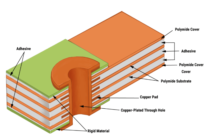
Flex pcb via
Advantages Of Using Flex PCB Vias In Modern Electronics
Flex PCB vias, or flexible printed circuit board vias, have become increasingly significant in the realm of modern electronics. These components offer a multitude of advantages that enhance the performance, reliability, and versatility of electronic devices. As technology continues to evolve, the demand for more compact, efficient, and durable electronic systems has driven the adoption of flex PCB vias, which play a crucial role in meeting these requirements.
One of the primary advantages of using flex PCB vias is their ability to facilitate complex interconnections within a compact space.
Traditional rigid PCBs often face limitations in terms of space and flexibility, which can hinder the design and functionality of electronic devices. Flex PCB vias, however, allow for the creation of intricate circuits that can bend and fold, enabling designers to maximize the use of available space. This is particularly beneficial in applications where space is at a premium, such as in wearable technology, medical devices, and compact consumer electronics.
In addition to space optimization, flex PCB vias contribute to enhanced reliability and durability.
The flexible nature of these vias allows them to withstand mechanical stress and vibrations that would typically damage rigid PCBs. This resilience is especially important in applications where electronic devices are subject to constant movement or harsh environmental conditions. For instance, in the automotive and aerospace industries, where components must endure extreme temperatures and mechanical shocks, flex PCB vias provide a robust solution that ensures long-term performance and reliability.
Moreover, the use of flex PCB vias can lead to significant cost savings in the manufacturing process.
By reducing the need for multiple rigid PCBs and connectors, manufacturers can streamline production and minimize material costs. The ability to integrate multiple functions into a single flexible circuit also reduces assembly time and labor costs. Consequently, the overall production process becomes more efficient, leading to faster time-to-market for new products.
Another notable advantage of flex PCB vias is their contribution to improved signal integrity and electrical performance.
The design flexibility offered by these vias allows for optimized routing of high-speed signals, minimizing issues such as signal loss, crosstalk, and electromagnetic interference. This is particularly critical in applications that require high-frequency signal transmission, such as telecommunications and data communication systems. By ensuring reliable signal transmission, flex PCB vias help maintain the integrity and performance of electronic devices.
Furthermore, the versatility of flex PCB vias extends to their compatibility with a wide range of materials and technologies.
They can be used in conjunction with various substrates, including polyimide and polyester, which offer excellent thermal and electrical properties. This compatibility allows for the development of customized solutions tailored to specific application requirements. Additionally, flex PCB vias can be integrated with advanced technologies such as surface mount devices (SMDs) and through-hole components, further enhancing their functionality and adaptability.
In conclusion, the advantages of using flex PCB vias in modern electronics are manifold. From space optimization and enhanced reliability to cost savings and improved signal integrity, these components offer a comprehensive solution that addresses the evolving demands of the electronics industry. As technology continues to advance, the adoption of flex PCB vias is likely to increase, driving innovation and enabling the development of more sophisticated and efficient electronic devices.
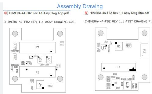
Design Considerations For Flex PCB Vias
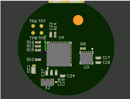
When designing flexible printed circuit boards (flex PCBs), one of the critical aspects to consider is the implementation of vias. Vias are essential components that establish electrical connections between different layers of a PCB.
In the context of flex PCBs, the design considerations for vias become even more crucial due to the unique mechanical and electrical properties of flexible substrates. Understanding these considerations can significantly impact the performance, reliability, and manufacturability of the final product.
To begin with, the choice of via type is a fundamental decision in flex PCB design.
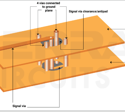
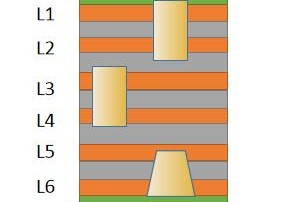
There are several types of vias, including through-hole vias, blind vias, and buried vias. Through-hole vias extend through the entire thickness of the PCB, while blind vias connect an outer layer to one or more inner layers without passing through the entire board. Buried vias, on the other hand, connect internal layers without reaching the outer surfaces. Each type has its advantages and limitations, and the selection depends on the specific requirements of the application. For instance, through-hole vias are generally more robust and easier to manufacture, but they may not be suitable for high-density designs where space is at a premium.
Another critical consideration is the via size and aspect ratio.
The aspect ratio, defined as the ratio of the via’s depth to its diameter, plays a significant role in determining the reliability of the via. A higher aspect ratio can lead to difficulties in plating the via walls uniformly, which may result in poor electrical performance and potential failure points. Therefore, it is essential to balance the via size and aspect ratio to ensure reliable electrical connections while maintaining the mechanical integrity of the flex PCB.
The material properties of the flex PCB substrate also influence via design.
Flexible substrates, such as polyimide, exhibit different thermal and mechanical characteristics compared to rigid substrates. These differences necessitate careful consideration of the thermal expansion coefficients and mechanical flexibility when designing vias. For example, the thermal expansion mismatch between the via plating material and the substrate can lead to stress concentrations, potentially causing via cracking or delamination. To mitigate these risks, designers often use materials with compatible thermal expansion properties and employ stress-relief techniques, such as teardrop pads, to distribute mechanical stresses more evenly.
Moreover, the placement and routing of vias must be strategically planned to avoid potential issues during the flexing and bending of the PCB.
Vias located in high-stress areas, such as bend regions, are more susceptible to mechanical fatigue and failure. Consequently, it is advisable to place vias in low-stress areas and use staggered or offset patterns to distribute mechanical loads more evenly. Additionally, incorporating redundant vias can enhance the reliability of critical connections by providing alternative current paths in case of via failure.
In addition to mechanical considerations, electrical performance is another vital aspect of via design in flex PCBs.
The parasitic inductance and capacitance associated with vias can affect signal integrity, especially in high-frequency applications. To minimize these effects, designers can use techniques such as via stitching, where multiple vias are placed in parallel to reduce inductance, or via-in-pad designs, which place vias directly within component pads to shorten signal paths and reduce parasitic elements.
In conclusion, the design considerations for flex PCB vias encompass a range of factors, including via type, size, aspect ratio, material properties, placement, and electrical performance. By carefully addressing these considerations, designers can optimize the performance, reliability, and manufacturability of flex PCBs, ensuring they meet the demanding requirements of modern electronic applications.
Manufacturing Challenges And Solutions For Flex PCB Vias
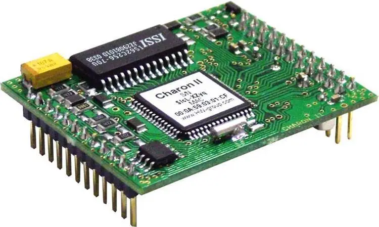
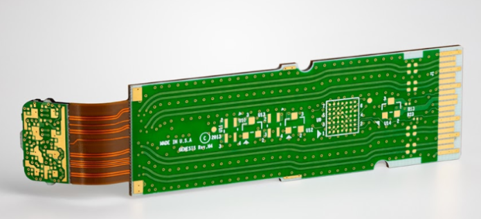
Flex PCBs, or flexible printed circuit boards, have become increasingly popular in various industries due to their ability to bend and conform to different shapes, making them ideal for compact and complex electronic devices. However, the manufacturing of flex PCBs presents unique challenges, particularly when it comes to the creation and implementation of vias. Vias, which are the electrical connections between different layers of a PCB, are crucial for the functionality of these circuits. The manufacturing challenges associated with flex PCB vias are multifaceted, but several solutions have been developed to address these issues effectively.
One of the primary challenges in manufacturing flex PCB vias is ensuring the mechanical reliability of the vias themselves.
Unlike rigid PCBs, flex PCBs are subject to constant bending and flexing, which can lead to mechanical stress on the vias. This stress can cause cracks or breaks in the vias, leading to circuit failure. To mitigate this issue, manufacturers often use advanced materials and techniques. For instance, the use of polyimide films, which are highly flexible and durable, can help absorb some of the mechanical stress. Additionally, the implementation of staggered vias, rather than stacked vias, can distribute the stress more evenly across the PCB, reducing the likelihood of failure.
Another significant challenge is the precision required in drilling the vias.
Flex PCBs are typically thinner than their rigid counterparts, making them more susceptible to damage during the drilling process. Laser drilling has emerged as a preferred method for creating vias in flex PCBs due to its high precision and minimal impact on the surrounding material. Laser drilling allows for the creation of very small vias, which is essential for high-density interconnect (HDI) designs. This method not only improves the accuracy of via placement but also reduces the risk of damaging the delicate flex PCB material.
The plating process for vias in flex PCBs also presents unique challenges.
Ensuring a uniform and reliable conductive layer within the via is critical for maintaining electrical connectivity. Traditional electroplating methods can be problematic due to the flexible nature of the substrate, which can lead to uneven plating and potential connectivity issues. To address this, manufacturers have turned to advanced plating techniques such as electroless plating, which provides a more uniform coating by depositing a thin layer of metal without the need for an electric current. This method ensures that the vias maintain consistent electrical performance even under the stress of flexing.
Thermal management is another critical aspect of manufacturing flex PCB vias.
The materials used in flex PCBs often have different thermal expansion coefficients compared to those used in rigid PCBs. This discrepancy can lead to thermal stress during the soldering process, potentially causing delamination or other forms of damage to the vias. To combat this, manufacturers employ specialized thermal management techniques, such as using low-temperature soldering materials and controlled cooling processes, to minimize thermal stress and ensure the integrity of the vias.
In conclusion, while the manufacturing of flex PCB vias presents several challenges, advancements in materials, drilling techniques, plating processes, and thermal management have provided effective solutions. By addressing these challenges, manufacturers can produce reliable and high-performance flex PCBs that meet the demands of modern electronic devices. The continuous evolution of these technologies promises to further enhance the capabilities and applications of flex PCBs in the future.
Applications Of Flex PCB Vias In Wearable Technology
Flex PCB vias, or flexible printed circuit board vias, are integral components in the design and functionality of modern wearable technology. These vias, which are essentially conductive pathways that connect different layers of a flexible PCB, enable the creation of compact, lightweight, and highly functional electronic devices. The applications of flex PCB vias in wearable technology are vast and varied, reflecting the growing demand for innovative and efficient electronic solutions in this rapidly evolving field.
One of the primary applications of flex PCB vias in wearable technology is in the development of smartwatches.
These devices require a high degree of flexibility and miniaturization to accommodate various sensors, processors, and communication modules within a limited space. Flex PCB vias facilitate the interconnection of these components, allowing for a seamless integration that enhances the overall performance and reliability of the smartwatch. Moreover, the flexibility of these vias ensures that the device can withstand the constant movement and bending associated with daily wear, thereby improving its durability and user experience.
In addition to smartwatches, flex PCB vias are also crucial in the design of fitness trackers.
These devices monitor various physiological parameters such as heart rate, steps taken, and calories burned, necessitating the incorporation of multiple sensors and data processing units. Flex PCB vias enable the efficient routing of electrical signals between these components, ensuring accurate data collection and real-time analysis. Furthermore, the lightweight nature of flexible PCBs, combined with the robustness of the vias, makes fitness trackers comfortable to wear for extended periods, thereby encouraging consistent use and promoting better health outcomes.
Another significant application of flex PCB vias is in the realm of medical wearables.
Devices such as continuous glucose monitors, wearable ECG monitors, and smart patches rely heavily on the advanced capabilities of flexible PCBs. The vias in these circuits allow for the precise and reliable transmission of critical health data, which is essential for timely diagnosis and intervention. Additionally, the biocompatibility and flexibility of these PCBs ensure that the medical wearables can be comfortably worn on the skin without causing irritation or discomfort, thereby enhancing patient compliance and the overall effectiveness of the device.
The integration of flex PCB vias is also evident in the development of augmented reality (AR) and virtual reality (VR) headsets.
These devices require a complex network of sensors, displays, and processing units to deliver immersive experiences. Flex PCB vias facilitate the compact and efficient design of these headsets, enabling the seamless transmission of data between various components. This not only enhances the performance and responsiveness of the AR/VR devices but also contributes to a more comfortable and ergonomic design, which is crucial for prolonged use.
Furthermore, the use of flex PCB vias extends to the realm of smart clothing.
These garments incorporate electronic components such as sensors, actuators, and communication modules to provide functionalities like biometric monitoring, environmental sensing, and even haptic feedback. Flex PCB vias enable the integration of these components into the fabric, allowing for the creation of smart clothing that is both functional and comfortable to wear. The flexibility and durability of these vias ensure that the electronic components can withstand the stresses of daily wear and washing, thereby extending the lifespan and utility of the smart clothing.
In conclusion, the applications of flex PCB vias in wearable technology are diverse and impactful. From smartwatches and fitness trackers to medical wearables, AR/VR headsets, and smart clothing, these vias play a crucial role in enabling the compact, flexible, and reliable design of modern wearable devices. As the demand for wearable technology continues to grow, the importance of flex PCB vias in driving innovation and enhancing user experience cannot be overstated.