Flexible Circuit Assembly Strategies for Next-Gen Electronics Design

Key Takeaways
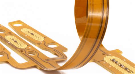
Modern flexible printed circuit assembly (FPCA) demands a strategic blend of advanced materials and precision manufacturing to meet the evolving needs of next-gen electronics. Innovations in PCB assembly (PCBA) now prioritize ultra-thin substrates and heat-resistant polymers, enabling circuits to withstand extreme bending and thermal stress. For IoT applications, miniaturized components and high-density interconnects are critical, ensuring seamless integration into compact, smart devices.
| Factor | Traditional PCBA | Next-Gen FPCA |
|---|---|---|
| Material Flexibility | Rigid FR-4 substrates | Polyimide or PET films |
| Component Density | Limited by board thickness | Up to 20% higher density |
| Production Speed | 8–12 hours per batch | 3–5 hours with laser ablation |
Furthermore, streamlined production efficiency is achieved through automated optical inspection (AOI) and robotic soldering, reducing defects by over 30% in wearable tech applications. Durability enhancements, such as conformal coatings and strain-relief designs, extend the lifecycle of flexible circuits in harsh environments. As industries shift toward IoT-integrated systems and foldable displays, optimizing PCBA workflows for scalability remains a cornerstone of next-gen electronics design.
Flex Circuit Assembly Innovations
The evolution of flexible printed circuit assembly is redefining how next-generation electronics are designed and manufactured. Central to these advancements is the integration of high-performance polymers and ultrathin conductive substrates, which enable circuits to withstand repeated bending without compromising electrical integrity. Modern PCBA processes now leverage laser direct imaging (LDI) and automated optical inspection (AOI) to achieve micron-level precision, ensuring reliable interconnects even in complex, multilayered designs.
A critical innovation lies in hybrid PCB assembly techniques that combine rigid-flex configurations with embedded components, reducing footprint while enhancing signal integrity for IoT and wearable applications. Manufacturers are adopting roll-to-roll (R2R) production systems to scale flexible circuit fabrication, slashing lead times by 30–40% compared to traditional batch processing. Simultaneously, advancements in anisotropic conductive films (ACFs) are streamlining the bonding of delicate sensors to flex substrates, a game-changer for medical wearables and foldable displays.
These breakthroughs not only address the mechanical challenges of dynamic bending environments but also align with sustainability goals through material-efficient designs. As industries push for thinner, lighter devices, the synergy between flexible PCBA methodologies and smart manufacturing platforms is setting new benchmarks for durability and energy efficiency in next-gen electronics.
Advanced Materials for Flex Circuit Reliability
The reliability of flexible printed circuit assembly hinges on the strategic use of advanced materials engineered to withstand mechanical stress, temperature fluctuations, and environmental factors. High-performance polymers like polyimide and liquid crystal polymer (LCP) are increasingly replacing traditional substrates due to their exceptional thermal stability, chemical resistance, and flexibility. These materials enable PCBA designs to maintain signal integrity even in dynamic applications such as foldable devices or wearable sensors.
For instance, adhesives with low coefficient of thermal expansion (CTE) are critical in minimizing delamination risks during PCB assembly, particularly in multi-layer configurations. Additionally, conductive inks infused with silver or graphene nanoparticles enhance trace durability while reducing impedance—a vital consideration for high-frequency IoT applications.
Tip: When selecting materials for flex circuit assembly, prioritize compatibility with both the manufacturing process (e.g., laser drilling) and end-use conditions (e.g., moisture exposure).
Innovations like ultra-thin copper cladding (≤5µm) further optimize weight and space efficiency without compromising conductivity. Combined with advanced encapsulation techniques, these materials ensure that flexible PCBA solutions meet rigorous industry standards for bend cycles (exceeding 200,000 cycles) and operational longevity. As next-gen electronics demand thinner, lighter, and more resilient circuits, material science remains the cornerstone of reliable flexible printed circuit assembly in cutting-edge applications.
Precision Manufacturing in Circuit Assembly
Achieving nanometer-level accuracy in flexible printed circuit assembly demands advanced PCB assembly techniques tailored for delicate substrates. Modern PCBA workflows now integrate laser direct imaging (LDI) systems to etch micro-scale traces on polyimide films, while automated optical inspection (AOI) ensures defect rates remain below 0.1%. For applications in medical devices or aerospace, robotic pick-and-place systems equipped with force-feedback mechanisms position components as small as 01005 packages without compromising the integrity of bendable circuits.
A critical advancement lies in adaptive soldering processes, where temperature profiles dynamically adjust to prevent warping in heat-sensitive materials. This precision extends to PCB assembly testing phases, with impedance-controlled testing rigs validating signal integrity across flex-rigid hybrid boards. Manufacturers are also adopting machine learning algorithms to predict and compensate for material expansion during lamination, reducing rework by up to 30%.
As IoT and wearable technologies demand thinner, lighter designs, PCBA providers prioritize modular tooling that accommodates rapid design iterations. By aligning with standards like IPC-A-610 for flex circuits, these strategies ensure reliability without sacrificing the production scalability required for next-gen electronics.
IoT Integration with Flexible Electronics
The rapid expansion of IoT-enabled devices demands electronics that balance compact design with robust functionality. Flexible printed circuit assembly (FPC assembly) plays a pivotal role here, enabling seamless integration into irregularly shaped sensors, wearables, and smart infrastructure. By leveraging advanced PCBA techniques, manufacturers can embed ultra-thin circuits into IoT systems without compromising signal integrity or durability.
A key advantage lies in the miniaturization of components. Flexible circuits, paired with high-density PCB assembly methods, allow for tighter component placement—critical for IoT devices requiring real-time data processing in confined spaces. Materials like polyimide substrates and conductive silver inks further enhance thermal stability and resistance to mechanical stress, ensuring reliability in dynamic environments such as industrial IoT or wearable health monitors.
To optimize IoT connectivity, PCBA workflows now incorporate hybrid rigid-flex designs, merging traditional rigid boards with flexible interconnects. This approach reduces points of failure while supporting wireless protocols like Bluetooth Low Energy or LoRaWAN. Additionally, automated optical inspection (AOI) during flexible circuit assembly ensures precision at scale, aligning with the demand for cost-effective, high-volume production.
As IoT ecosystems grow, the synergy between energy-efficient designs and flexible electronics will drive innovations in edge computing and sustainable device lifecycle management.
Streamlining Flex Circuit Production Efficiency
Achieving optimal efficiency in flexible printed circuit assembly requires balancing precision with scalable manufacturing processes. Modern PCB assembly techniques leverage automated optical inspection (AOI) and laser direct imaging (LDI) to minimize defects while accelerating throughput. For PCBA workflows, integrating surface-mount technology (SMT) with flexible substrates ensures consistent component placement, even for ultra-thin designs.
A critical focus lies in reducing material waste through dynamic panelization, which optimizes substrate usage without compromising circuit integrity. Advanced IoT-enabled monitoring systems further enhance efficiency by tracking real-time production metrics, enabling rapid adjustments to temperature, pressure, and alignment parameters. This data-driven approach not only cuts downtime but also aligns with lean manufacturing principles.
Collaboration between PCB assembly engineers and material scientists is vital for selecting adhesives and coatings that withstand high-speed assembly lines. By standardizing design-for-manufacturing (DFM) guidelines for PCBA, teams can preemptively address challenges like impedance mismatches or thermal expansion disparities. Such strategies ensure seamless transitions from prototyping to mass production, setting the stage for scalable integration with IoT and wearable ecosystems discussed in subsequent sections.
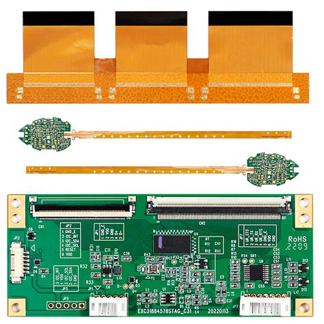
Wearable Tech and Flex Circuit Integration
The rapid evolution of wearable technology demands electronics that conform to dynamic, space-constrained geometries while maintaining robust performance. Flexible printed circuit assembly (flex PCBA) has emerged as a cornerstone for these applications, enabling seamless integration into curved surfaces, stretchable bands, and ultra-thin devices. Unlike traditional PCB assembly methods, which rely on rigid substrates, flex PCBA leverages lightweight, bendable materials like polyimide to withstand repeated mechanical stress without compromising electrical integrity.
Critical to this integration is the optimization of pcb assembly processes for miniaturized components. Advanced techniques such as laser-drilled microvias and ultra-fine-pitch soldering ensure reliable interconnections in densely packed wearables, from fitness trackers to medical sensors. Designers must also account for environmental factors—moisture resistance, thermal cycling, and biocompatibility—to meet the stringent demands of skin-contact devices.
Moreover, the convergence of IoT-enabled functionalities and flexible circuit assembly introduces new challenges in power management and signal integrity. Innovations like stretchable conductive inks and hybrid rigid-flex designs are bridging this gap, allowing sensors and antennas to coexist on the same substrate. By aligning pcba workflows with wearable-specific requirements—such as low-profile connectors and energy-efficient layouts—manufacturers can accelerate prototyping cycles while maintaining scalability for mass production.
As wearables expand into healthcare, AR/VR, and smart textiles, the synergy between material science and flexible circuit assembly will remain pivotal in delivering devices that are both durable and imperceptibly integrated into daily life.
Enhancing Durability in Flexible Electronics
As flexible electronics evolve to meet the demands of IoT and wearable devices, ensuring long-term durability remains a critical challenge. Advanced PCB assembly (PCBA) techniques now prioritize materials engineered for resilience, such as polyimide substrates and stretchable conductive inks, which maintain conductivity under repeated bending. Manufacturers are adopting laser ablation and automated optical inspection to minimize microcracks during flex circuit assembly, a common failure point in dynamic applications.
To enhance mechanical stability, adhesive bonding methods are being refined to withstand thermal cycling and moisture exposure—key stressors in automotive and medical electronics. Innovations in PCBA workflows, including conformal coatings with nano-enhanced polymers, further protect circuits from environmental degradation. Additionally, accelerated life testing simulates years of flexing in days, enabling engineers to identify weaknesses before scaling production.
These strategies align with the broader shift toward miniaturization and high-density interconnects in next-gen designs. By integrating robust materials with precision PCB assembly processes, developers can deliver flexible electronics that endure harsh operating conditions without compromising performance—a necessity for applications ranging from foldable displays to implantable sensors.

Future Trends in Next-Gen Circuit Design
Emerging technologies are driving transformative shifts in flexible printed circuit assembly, with PCB assembly methodologies adapting to support ultra-compact, multifunctional designs. The integration of PCBA processes with stretchable conductive inks and nanostructured substrates is enabling circuits that maintain performance under extreme mechanical stress, critical for foldable displays and implantable medical devices.
A key development lies in hybrid architectures combining traditional rigid PCB assembly techniques with flexible interconnects, allowing seamless integration of sensors and power modules in IoT ecosystems. Advanced simulation tools now optimize material selection and trace routing prior to PCBA, reducing prototyping iterations by 40% while ensuring signal integrity in curved configurations.
The rise of edge computing demands self-healing circuit designs that leverage AI-driven PCBA workflows to predict and mitigate flex fatigue. Innovations like laser-direct structuring (LDS) are enabling 3D-molded circuits with embedded components, eliminating wiring constraints in wearable tech. Sustainability trends are pushing adoption of biodegradable flex films compatible with standard PCB assembly lines, aligning with circular manufacturing principles.
As 6G connectivity emerges, terahertz-frequency flexible circuits will require novel PCBA approaches to manage signal loss in dynamic bending scenarios. These advancements position flexible electronics as the backbone for next-gen applications, from morphing automotive dashboards to adaptive aerospace systems.
Conclusion
The evolution of flexible printed circuit assembly underscores its pivotal role in advancing next-generation electronics. By integrating advanced materials like polyimide substrates and conductive inks, manufacturers achieve unprecedented reliability in pcb assembly for applications ranging from wearables to IoT devices. The shift toward precision manufacturing techniques, such as laser ablation and automated optical inspection (AOI), ensures consistent quality in pcba processes while minimizing defects.
As industries prioritize miniaturization and energy efficiency, optimizing flexible circuit production becomes critical. Innovations in roll-to-roll processing and modular design frameworks streamline workflows, reducing time-to-market for complex electronics. Moreover, the synergy between durable flexible circuits and emerging technologies—like 5G and edge computing—creates opportunities for smarter, lighter devices.
Looking ahead, the convergence of pcb assembly standards with sustainable practices will define the next phase of growth. By balancing cost-efficiency with performance demands, manufacturers can meet the escalating requirements of medical, automotive, and consumer tech sectors. Ultimately, the success of flexible electronics hinges on continuous collaboration between material scientists, engineers, and smart manufacturing ecosystems to push the boundaries of what’s possible.
Frequently Asked Questions
What distinguishes flexible printed circuit assembly from traditional PCB assembly?
Flexible circuits use polyimide or PET substrates instead of rigid materials, enabling bending and folding. While PCBA (Printed Circuit Board Assembly) for rigid boards focuses on component density, flexible designs prioritize dynamic stress resistance and lightweight integration.
How do advanced materials enhance reliability in flexible PCB assembly?
Materials like liquid crystal polymer (LCP) and adhesiveless copper laminates minimize thermal expansion mismatches. These innovations reduce solder joint fatigue in PCBA, ensuring stability in high-vibration environments like wearables or automotive systems.
Can flexible circuits support IoT and wearable device requirements?
Yes. Their thin profile and conformal shaping allow seamless integration into compact, curved IoT sensors and medical wearables. PCB assembly techniques like laser drilling and ultra-fine pitch soldering enable high-density interconnects for embedded sensors.
What strategies optimize production efficiency in flexible PCBA?
Automated optical inspection (AOI) and roll-to-roll manufacturing reduce manual handling. Pairing 3D printing for rapid prototyping with modular PCB assembly workflows cuts lead times by 30–40% for high-mix batches.
Are flexible circuits cost-effective for low-volume projects?
Advances in digital tooling and panelization algorithms now make small-batch flexible PCB assembly viable. Hybrid designs combining rigid and flexible sections (rigid-flex PCBA) further balance cost and performance.
Explore Custom Solutions for Your Flex Circuit Needs
For tailored PCB assembly strategies or PCBA prototyping support, please click here to connect with our engineering team.