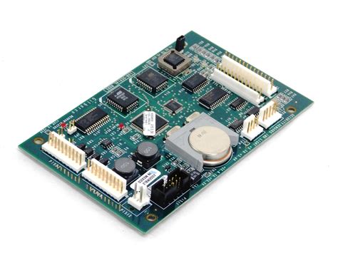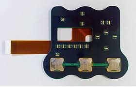
Flexible membrane pcb
Advantages Of Using Flexible Membrane PCBs In Modern Electronics
Flexible membrane printed circuit boards (PCBs) have emerged as a pivotal component in the realm of modern electronics, offering a multitude of advantages that cater to the evolving demands of contemporary technology. As electronic devices become increasingly compact and sophisticated, the need for adaptable and efficient circuit solutions has never been more pronounced. Flexible membrane PCBs, with their unique properties, provide an ideal solution to these challenges, thereby playing a crucial role in the advancement of electronic design and functionality.
One of the primary advantages of flexible membrane PCBs is their inherent adaptability.
Unlike traditional rigid PCBs, flexible membranes can be bent, folded, and twisted without compromising their functionality. This flexibility allows for innovative design possibilities, enabling engineers to create more compact and lightweight devices. As a result, flexible membrane PCBs are particularly beneficial in applications where space is at a premium, such as in wearable technology, medical devices, and portable electronics. By facilitating the integration of complex circuits into confined spaces, these PCBs contribute significantly to the miniaturization trend in modern electronics.
In addition to their adaptability, flexible membrane PCBs offer enhanced durability and reliability.
The materials used in their construction, such as polyimide or polyester films, are known for their resilience and resistance to environmental stressors. This makes flexible PCBs less susceptible to damage from vibrations, shocks, and temperature fluctuations, which are common in various electronic applications. Consequently, devices that incorporate flexible membrane PCBs tend to have a longer operational lifespan and require less frequent maintenance, thereby reducing overall costs and improving user satisfaction.
Moreover, the lightweight nature of flexible membrane PCBs is another compelling advantage.
As electronic devices become more portable, reducing weight without sacrificing performance is a critical consideration. Flexible PCBs contribute to this goal by offering a lightweight alternative to traditional circuit boards, without compromising on electrical performance. This characteristic is particularly advantageous in the development of mobile devices, drones, and other applications where weight is a critical factor.
Furthermore, flexible membrane PCBs facilitate improved electrical performance due to their ability to reduce the number of interconnects required in a circuit.
By minimizing the need for connectors and solder joints, these PCBs help decrease the potential for signal loss and interference, leading to more efficient and reliable electronic systems. This is especially important in high-frequency applications, where maintaining signal integrity is paramount.
In addition to these technical benefits, flexible membrane PCBs also offer economic advantages.
The manufacturing process for these PCBs can be more cost-effective than that of rigid boards, particularly for complex designs that require multiple layers. The ability to produce flexible PCBs in a roll-to-roll process further enhances their cost-effectiveness, making them an attractive option for large-scale production.
In conclusion, the advantages of using flexible membrane PCBs in modern electronics are manifold. Their adaptability, durability, lightweight nature, and improved electrical performance make them an indispensable component in the design and development of cutting-edge electronic devices. As technology continues to advance, the role of flexible membrane PCBs is likely to expand, driving further innovation and enabling the creation of even more sophisticated and efficient electronic solutions.

Design Considerations For Flexible Membrane PCBs
When designing flexible membrane PCBs, several critical considerations must be taken into account to ensure optimal performance and reliability. These unique circuit boards, characterized by their ability to bend and conform to various shapes, are increasingly used in applications where space constraints and dynamic movement are prevalent. As such, understanding the nuances of their design is essential for engineers and designers aiming to leverage their full potential.
To begin with, material selection is a fundamental aspect of designing flexible membrane PCBs.
The choice of substrate material significantly influences the board’s flexibility, durability, and thermal performance. Polyimide is a popular choice due to its excellent thermal stability and mechanical properties, which make it suitable for a wide range of applications. However, other materials like polyester may be used in cost-sensitive applications where extreme thermal resistance is not a primary concern. The selection process should carefully consider the specific environmental conditions the PCB will encounter, such as temperature fluctuations and exposure to chemicals.
In addition to material selection, the layout design of flexible membrane PCBs requires meticulous attention.
Unlike rigid PCBs, flexible circuits must accommodate bending and flexing without compromising the integrity of the conductive traces. Therefore, it is crucial to design trace patterns that minimize stress concentration. Utilizing curved traces instead of sharp angles can help distribute mechanical stress more evenly, reducing the risk of trace cracking. Furthermore, maintaining a consistent trace width and spacing is vital to prevent impedance variations, which can affect signal integrity.
Transitioning from layout design to the consideration of component placement, it is important to recognize that the placement of components on a flexible membrane PCB can significantly impact its performance.
Components should be strategically positioned to avoid areas of high mechanical stress, such as bend lines. Placing components in these areas can lead to solder joint failure or component detachment over time. Additionally, designers should consider the use of surface-mount technology (SMT) components, which are generally more suitable for flexible applications due to their lower profile and lighter weight compared to through-hole components.
Moreover, the choice of adhesive and protective coatings plays a pivotal role in the longevity and reliability of flexible membrane PCBs.
Adhesives are used to bond the layers of the PCB together, and selecting the right adhesive is crucial for maintaining flexibility while ensuring strong adhesion. Protective coatings, such as conformal coatings, provide an additional layer of protection against environmental factors like moisture and dust. These coatings must be carefully selected to ensure they do not impede the flexibility of the PCB.
Finally, testing and validation are indispensable steps in the design process of flexible membrane PCBs.
Given their unique properties and applications, these PCBs must undergo rigorous testing to ensure they meet the required performance standards. Flex testing, thermal cycling, and environmental testing are some of the critical assessments that help identify potential failure points and validate the design’s robustness.
In conclusion, designing flexible membrane PCBs involves a comprehensive understanding of material properties, layout design, component placement, and protective measures. By carefully considering these factors, designers can create flexible circuits that not only meet the demands of their specific applications but also offer enhanced reliability and performance. As technology continues to advance, the role of flexible membrane PCBs is likely to expand, making these design considerations increasingly important for future innovations.
Applications Of Flexible Membrane PCBs In Wearable Technology
Flexible membrane printed circuit boards (PCBs) have emerged as a pivotal component in the rapidly evolving field of wearable technology. These innovative circuits offer a unique combination of flexibility, durability, and lightweight properties, making them ideal for integration into wearable devices. As the demand for more sophisticated and user-friendly wearables grows, the applications of flexible membrane PCBs continue to expand, offering new possibilities for both consumers and industries.
One of the primary applications of flexible membrane PCBs in wearable technology is in the realm of health monitoring devices.
These devices, which include fitness trackers and smartwatches, rely heavily on the adaptability of flexible PCBs to conform to the contours of the human body. This adaptability ensures that sensors maintain optimal contact with the skin, thereby providing accurate and reliable data. For instance, heart rate monitors and electrocardiogram (ECG) sensors embedded in wearables benefit from the precise fit that flexible PCBs offer, enhancing the overall performance of these health monitoring systems.
In addition to health monitoring, flexible membrane PCBs are instrumental in the development of smart clothing.
This innovative application involves embedding electronic components directly into fabrics, creating garments that can perform a variety of functions. From monitoring physiological parameters to providing haptic feedback, smart clothing leverages the flexibility and thin profile of membrane PCBs to seamlessly integrate technology into everyday wear. This integration not only enhances the functionality of clothing but also opens up new avenues for fashion and design, allowing for the creation of garments that are both stylish and technologically advanced.
Moreover, flexible membrane PCBs are crucial in the advancement of augmented reality (AR) and virtual reality (VR) wearables.
Devices such as AR glasses and VR headsets require intricate circuitry that can accommodate complex functionalities while maintaining a lightweight and comfortable design. Flexible PCBs meet these requirements by providing a platform that supports high-density interconnections and complex circuitry without adding significant bulk. This capability is essential for ensuring that AR and VR devices deliver immersive experiences without compromising user comfort.
Furthermore, the use of flexible membrane PCBs extends to the development of medical wearables, which are designed to assist in patient care and monitoring.
These devices, which can range from insulin pumps to wearable defibrillators, benefit from the reliability and resilience of flexible PCBs. The ability to withstand bending and twisting without losing functionality is particularly important in medical applications, where device failure can have serious consequences. By incorporating flexible PCBs, medical wearables can offer continuous monitoring and timely interventions, thereby improving patient outcomes.
In conclusion, the applications of flexible membrane PCBs in wearable technology are vast and varied, encompassing health monitoring, smart clothing, AR and VR devices, and medical wearables. As technology continues to advance, the role of flexible PCBs in wearables is likely to expand further, driven by the need for devices that are not only functional but also comfortable and unobtrusive. The unique properties of flexible membrane PCBs make them an indispensable component in the design and development of next-generation wearable technology, promising a future where technology is seamlessly integrated into our daily lives.
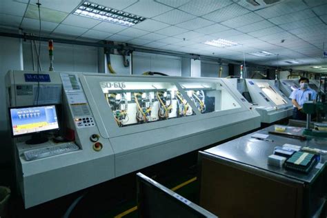
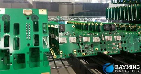
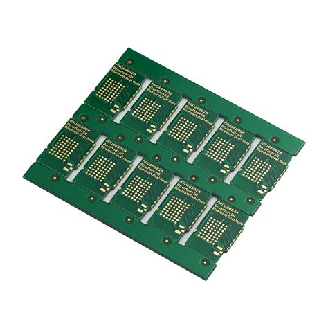
Manufacturing Process Of Flexible Membrane PCBs
The manufacturing process of flexible membrane printed circuit boards (PCBs) is a sophisticated and intricate procedure that requires precision and expertise. Flexible membrane PCBs are essential components in a wide range of electronic devices, offering the advantage of being lightweight, thin, and capable of bending to fit into compact spaces. The process begins with the selection of appropriate materials, which is crucial for ensuring the durability and functionality of the final product. Typically, polyimide or polyester films are chosen due to their excellent thermal stability and flexibility. These materials serve as the substrate upon which the circuit is built.
Once the substrate is selected, the next step involves the application of a conductive material, usually copper, onto the flexible film.
This is achieved through a process known as electroless plating, where a thin layer of copper is deposited onto the substrate without the use of an electric current. This initial layer serves as a foundation for further copper buildup. Following this, the substrate undergoes a photolithographic process, which is pivotal in defining the circuit pattern. A photoresist material is applied to the copper-coated substrate, and ultraviolet light is used to transfer the desired circuit pattern onto the photoresist. The areas exposed to light become hardened, while the unexposed areas remain soft and are subsequently removed, revealing the underlying copper.
The next phase involves the etching process, where the exposed copper is chemically removed, leaving behind the desired circuit pattern.
This step is critical, as it determines the precision and accuracy of the circuit design. After etching, the remaining photoresist is stripped away, exposing the clean copper circuit. To enhance the durability and conductivity of the circuit, additional layers of copper may be electroplated onto the existing pattern. This step not only strengthens the circuit but also ensures optimal electrical performance.
Following the formation of the circuit, the flexible membrane PCB undergoes a series of finishing processes
These include the application of a solder mask, which serves to protect the copper traces from oxidation and prevents solder bridges during component assembly. The solder mask is typically applied as a liquid and then cured to form a protective layer. Additionally, a surface finish, such as immersion gold or silver, may be applied to the exposed copper pads to enhance solderability and protect against corrosion.
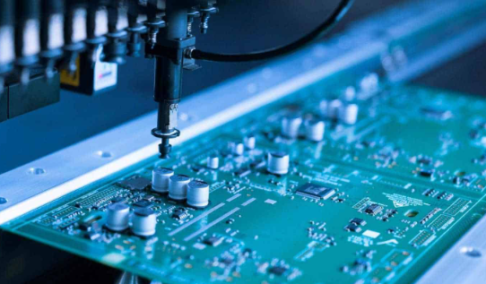
The final stages of the manufacturing process involve the assembly and testing of the flexible membrane PCB.
Components are mounted onto the circuit using surface mount technology (SMT) or through-hole technology, depending on the design requirements. Once assembled, the PCB undergoes rigorous testing to ensure its functionality and reliability. This includes electrical testing to verify circuit continuity and performance, as well as environmental testing to assess the PCB’s resilience under various conditions.
In conclusion, the manufacturing process of flexible membrane PCBs is a meticulous and highly technical endeavor that demands careful attention to detail at every stage. From material selection to final testing, each step is crucial in producing a high-quality, reliable product that meets the demands of modern electronic applications. The ability of flexible membrane PCBs to conform to complex shapes and withstand challenging environments makes them indispensable in the ever-evolving landscape of electronic design and innovation.