flexible pcb bend radius
Understanding The Importance Of Bend Radius In Flexible PCBs
In the realm of modern electronics, flexible printed circuit boards (PCBs) have emerged as a pivotal innovation, offering unparalleled versatility and adaptability.
These flexible PCBs are integral to a wide array of applications, from wearable technology to sophisticated aerospace systems. However, to harness their full potential, it is crucial to understand the concept of bend radius, a fundamental aspect that significantly influences the performance and reliability of flexible PCBs.
The bend radius of a flexible PCB refers to the minimum radius that the board can be bent without causing damage to its conductive pathways or compromising its structural integrity.
This parameter is essential because it dictates how the PCB can be integrated into various devices, especially those with limited space or requiring dynamic movement. A well-calculated bend radius ensures that the PCB can withstand repeated flexing and bending without failure, thereby extending its operational lifespan.
To comprehend the importance of bend radius, one must first consider the materials used in flexible PCBs.
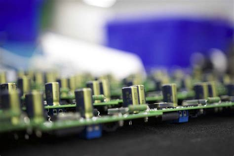
These boards are typically composed of a flexible substrate, such as polyimide, which provides the necessary pliability. The conductive traces, often made of copper, are laminated onto this substrate. When a flexible PCB is bent, the outer layers experience tensile stress, while the inner layers undergo compressive stress. If the bend radius is too small, these stresses can exceed the material’s tolerance, leading to cracks or breaks in the conductive traces.
Moreover, the bend radius is not a one-size-fits-all parameter; it varies depending on several factors, including the thickness of the PCB, the materials used, and the specific application requirements.
For instance, a thicker PCB will generally require a larger bend radius to prevent damage, while a thinner board can accommodate a tighter bend. Additionally, the presence of components on the PCB can further influence the bend radius, as these components may add rigidity or require additional clearance.
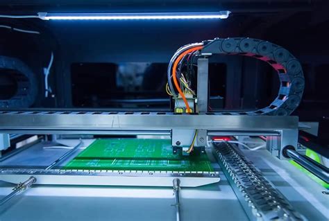
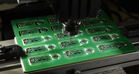
Understanding the bend radius is also crucial for the design and manufacturing processes of flexible PCBs.
During the design phase, engineers must carefully calculate the appropriate bend radius to ensure that the PCB can be integrated seamlessly into the final product. This involves considering not only the physical constraints of the device but also the environmental conditions it will encounter, such as temperature fluctuations and mechanical vibrations. In the manufacturing phase, precise control over the bend radius is necessary to maintain quality and consistency across production batches.
Furthermore, the bend radius has implications for the testing and validation of flexible PCBs.
Rigorous testing is essential to verify that the PCB can endure the expected bending and flexing cycles without degradation. This testing often involves subjecting the PCB to repeated bending at various angles and radii to simulate real-world conditions. By doing so, manufacturers can identify potential failure points and make necessary adjustments to the design or materials.
In conclusion, the bend radius is a critical factor in the design, manufacturing, and application of flexible PCBs. It ensures that these versatile components can perform reliably in diverse environments and applications. By understanding and optimizing the bend radius, engineers and manufacturers can unlock the full potential of flexible PCBs, paving the way for innovative electronic solutions that meet the demands of an ever-evolving technological landscape.
Design Guidelines For Optimizing Flexible PCB Bend Radius
When designing flexible printed circuit boards (PCBs), one of the critical considerations is the bend radius, which significantly impacts the board’s performance and longevity. The bend radius refers to the minimum radius a flexible PCB can be bent without causing damage or compromising its functionality. Understanding and optimizing this parameter is essential for engineers and designers aiming to create reliable and efficient flexible circuits.
To begin with, the bend radius is influenced by several factors, including the materials used, the thickness of the PCB, and the number of layers.
Typically, a larger bend radius is recommended to minimize stress on the circuit, thereby reducing the risk of fractures or delamination. For single-layer flexible PCBs, a bend radius of at least ten times the thickness of the material is generally advised. In contrast, multilayer flexible PCBs may require a bend radius of up to twenty times the thickness, depending on the specific application and material properties.
Moreover, the choice of materials plays a pivotal role in determining the optimal bend radius.
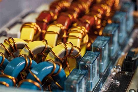
Polyimide is a popular substrate material for flexible PCBs due to its excellent thermal stability and mechanical properties. However, the copper used for the conductive traces also affects flexibility. Thinner copper layers can enhance flexibility but may require careful handling to prevent damage during manufacturing and assembly. Therefore, balancing material selection with design requirements is crucial for achieving the desired bend radius.
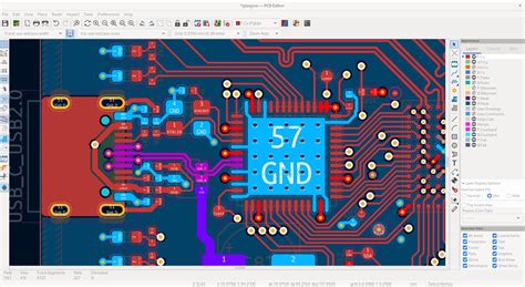
In addition to material considerations, the layout and routing of traces on the flexible PCB can significantly influence the bend radius.
Designers should aim to minimize the number of vias and avoid placing components or traces near the bend area. This approach helps distribute stress more evenly across the board, reducing the likelihood of mechanical failure. Furthermore, using curved traces instead of sharp angles can enhance flexibility and improve the board’s ability to withstand repeated bending.
Another important aspect to consider is the environment in which the flexible PCB will operate.
Factors such as temperature fluctuations, humidity, and exposure to chemicals can affect the board’s performance and durability. Therefore, it is essential to account for these environmental conditions when determining the appropriate bend radius. For instance, in high-temperature applications, a larger bend radius may be necessary to accommodate thermal expansion and contraction without causing damage to the circuit.
Testing and simulation are invaluable tools in optimizing the bend radius of flexible PCBs.
By employing finite element analysis (FEA) and other simulation techniques, designers can predict how the board will behave under various bending conditions. This predictive capability allows for adjustments to be made early in the design process, reducing the risk of costly revisions later on. Additionally, physical testing of prototypes can provide real-world insights into the board’s performance, ensuring that the final product meets the required specifications.
In conclusion, optimizing the bend radius of flexible PCBs is a multifaceted process that requires careful consideration of materials, design, and environmental factors. By adhering to established guidelines and leveraging advanced simulation and testing methods, designers can create flexible circuits that are both reliable and efficient. As technology continues to evolve, the demand for flexible PCBs will likely increase, making the understanding of bend radius optimization even more critical for future innovations.
Common Mistakes To Avoid With Flexible PCB Bend Radius
When designing flexible printed circuit boards (PCBs), understanding the intricacies of bend radius is crucial to ensuring both functionality and longevity. A common mistake in flexible PCB design is underestimating the importance of the bend radius, which can lead to mechanical failures and compromised electrical performance. The bend radius is the minimum radius one can bend a flexible PCB without causing damage. It is essential to consider this factor during the design phase to avoid costly errors and ensure the reliability of the final product.
One frequent error is neglecting to account for the material properties of the flexible PCB.
Different materials have varying degrees of flexibility and tensile strength, which directly impact the bend radius. For instance, polyimide, a popular material for flexible PCBs, offers excellent flexibility but still requires careful consideration of its limits. Designers must ensure that the chosen material can withstand the intended bending without cracking or delaminating. Therefore, it is imperative to consult material datasheets and manufacturer guidelines to determine the appropriate bend radius for the specific material in use.
Another mistake often encountered is the oversight of the copper layer thickness.
The thickness of the copper traces on a flexible PCB significantly influences the bend radius. Thicker copper layers are less flexible and require a larger bend radius to prevent cracking. Designers should aim to use the thinnest copper layer possible that still meets the electrical requirements of the circuit. By doing so, they can achieve a smaller bend radius, enhancing the flexibility of the PCB. Additionally, it is advisable to use rolled annealed copper instead of electro-deposited copper, as the former offers better flexibility and is less prone to cracking under stress.
Furthermore, improper trace routing can exacerbate issues related to bend radius.
Traces that run perpendicular to the bend can experience significant stress, leading to potential breaks or fractures. To mitigate this risk, designers should route traces parallel to the bend whenever possible. This orientation reduces the stress on the traces and helps maintain the integrity of the circuit. Moreover, incorporating curved traces instead of sharp angles can further alleviate stress concentrations, promoting a more robust design.
In addition to these considerations, it is crucial to avoid placing components or vias too close to the bend area.
Components and vias can create stress points that increase the likelihood of mechanical failure. By maintaining a safe distance from the bend, designers can prevent undue stress on these elements, thereby enhancing the durability of the flexible PCB. It is also beneficial to use staggered vias rather than stacked ones, as this configuration distributes stress more evenly across the board.
Lastly, failing to conduct thorough testing and simulation can lead to unforeseen issues with the bend radius.
Advanced simulation tools allow designers to model the mechanical behavior of flexible PCBs under various conditions, providing valuable insights into potential problem areas. By leveraging these tools, designers can identify and address issues before they manifest in physical prototypes, saving time and resources.
In conclusion, avoiding common mistakes related to flexible PCB bend radius requires a comprehensive understanding of material properties, copper thickness, trace routing, component placement, and thorough testing. By addressing these factors during the design phase, engineers can create flexible PCBs that are both reliable and efficient, ultimately leading to successful product development.
Innovations In Flexible PCB Technology: Reducing Bend Radius Constraints
In recent years, the electronics industry has witnessed significant advancements in flexible printed circuit board (PCB) technology, particularly in the realm of reducing bend radius constraints. This innovation is pivotal as it enhances the versatility and application of flexible PCBs in various sectors, including consumer electronics, medical devices, and automotive industries.
The bend radius of a flexible PCB refers to the minimum radius that the board can be bent without causing damage or compromising its functionality. Traditionally, this has been a limiting factor in the design and application of flexible circuits. However, recent technological advancements have begun to address these limitations, offering new possibilities for engineers and designers.
One of the primary factors contributing to the reduction in bend radius constraints is the development of new materials.
These materials are engineered to provide greater flexibility and durability, allowing the PCBs to withstand tighter bends without experiencing mechanical failure. For instance, the use of polyimide films and advanced copper foils has been instrumental in achieving smaller bend radii. These materials not only offer superior flexibility but also maintain excellent electrical performance, which is crucial for the reliability of electronic devices.
Moreover, innovations in manufacturing processes have played a significant role in reducing bend radius constraints.
Techniques such as laser direct structuring and additive manufacturing have enabled the production of more intricate and flexible circuit designs. These processes allow for precise control over the thickness and composition of the PCB layers, which is essential for achieving a smaller bend radius. Additionally, advancements in adhesive technologies have improved the bonding strength between layers, further enhancing the flexibility and resilience of the boards.
Another critical aspect of reducing bend radius constraints is the design optimization of flexible PCBs.
Engineers are now employing sophisticated simulation tools to model the mechanical behavior of flexible circuits under various conditions. These tools enable designers to predict potential stress points and optimize the layout to minimize mechanical strain. By strategically placing components and routing traces, designers can significantly reduce the risk of damage when the board is bent. This approach not only improves the durability of the PCB but also expands its potential applications in compact and dynamic environments.
Furthermore, the integration of flexible PCBs with other emerging technologies is opening new avenues for innovation.
For example, the combination of flexible circuits with wearable technology has led to the development of more comfortable and adaptable devices. These devices can conform to the contours of the human body, providing enhanced functionality and user experience. Similarly, in the automotive industry, flexible PCBs are being used to create more efficient and lightweight electronic systems, contributing to the development of smarter and more sustainable vehicles.
In conclusion, the reduction of bend radius constraints in flexible PCB technology represents a significant advancement with far-reaching implications. Through the development of new materials, innovative manufacturing processes, and optimized design strategies, the electronics industry is overcoming traditional limitations and unlocking new possibilities for flexible circuits. As these technologies continue to evolve, it is anticipated that flexible PCBs will play an increasingly vital role in the advancement of electronic devices across various sectors, driving innovation and enhancing the capabilities of modern technology.