Flextronics PCB Reliability in Advanced Assembly Processes
Key Takeaways
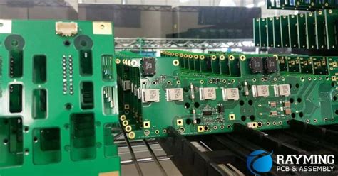
When evaluating PCB manufacturing solutions for advanced assembly, you’ll find that leading PCB manufacturing companies prioritize defect prevention and process optimization to ensure reliability. Flextronics’ approach integrates proprietary techniques like automated optical inspection (AOI) and real-time thermal profiling to minimize errors during high-density PCB assembly. These strategies directly address challenges in high-performance computing and cloud infrastructure applications, where even minor defects can compromise system integrity.
To balance PCB manufacturing cost with quality, Flextronics employs a tiered testing framework:
| Testing Phase | Methodology | Outcome |
|---|---|---|
| Pre-Assembly | Material Stress Analysis | Identifies substrate vulnerabilities |
| In-Process | AOI + X-Ray Inspection | Detects micro-defects in real-time |
| Post-Assembly | HAST (Highly Accelerated Stress) | Validates long-term reliability |
“In cloud infrastructure, PCB reliability isn’t optional—it’s the foundation of uptime.” — Senior Engineer, Flextronics Whitepaper
For PCB manufacturing business stakeholders, optimizing assembly workflows reduces rework rates by up to 40%, as seen in Flextronics’ deployment of predictive analytics for solder paste application. This precision ensures compatibility with high-density designs, critical for AI/ML hardware and 5G infrastructure. By prioritizing rigorous testing methodologies, you mitigate risks while scaling production—a balance often overlooked in cost-driven PCB manufacturing environments.
Flextronics PCB Defect Prevention Strategies
To minimize risks in PCB manufacturing, Flextronics employs a multi-layered approach that integrates advanced analytics with process standardization. By leveraging real-time monitoring systems, anomalies in material behavior or assembly conditions are detected early, reducing the likelihood of defects in high-density designs. For PCB manufacturing companies, controlling PCB manufacturing cost while maintaining quality requires balancing precision tooling with optimized workflows—a core focus in Flextronics’ proprietary methodologies.
Their defect prevention framework includes predictive modeling to simulate thermal and mechanical stresses, ensuring designs meet reliability thresholds before production begins. This proactive strategy not only addresses common failure points in PCB manufacturing business operations but also aligns with stringent requirements for cloud infrastructure and high-performance computing applications. Cross-functional teams validate each stage, from solder paste application to component placement, using automated optical inspection (AOI) to eliminate human error.
By prioritizing data-driven adjustments, Flextronics sustains defect rates below industry averages—critical for applications demanding zero tolerance for downtime. This systematic approach ensures scalability for clients navigating evolving PCB manufacturing demands without compromising on traceability or yield rates.

Optimizing Flextronics PCB Assembly Processes
When refining PCB manufacturing workflows, you need solutions that balance precision with scalability. Flextronics achieves this through process-driven optimizations that address both PCB manufacturing cost and quality. By implementing proprietary solder paste application techniques and automated optical inspection (AOI) systems, they minimize defects while maintaining throughput—critical for PCB manufacturing companies serving time-sensitive industries like high-performance computing.
Advanced thermal management protocols ensure consistent performance in high-density applications, reducing rework cycles that inflate operational expenses. This approach directly impacts the PCB manufacturing business by enabling tighter tolerances for complex designs, such as those used in cloud infrastructure environments. Real-time data analytics further streamline material usage, cutting waste without compromising reliability.
To sustain competitiveness, Flextronics integrates machine learning algorithms into assembly line diagnostics, predicting potential bottlenecks before they disrupt production. Such innovations not only enhance yield rates but also create cost efficiencies that benefit clients managing large-scale deployments. By aligning PCB manufacturing methodologies with evolving industry demands, they deliver assemblies that meet both technical specifications and economic objectives.

High-Performance Computing PCB Reliability
When designing systems for high-performance computing (HPC), ensuring PCB reliability becomes non-negotiable. These applications demand ultra-low latency, thermal stability, and consistent signal integrity under extreme workloads. To meet these requirements, PCB manufacturing companies prioritize advanced materials like low-loss dielectrics and high-Tg laminates, which minimize signal degradation even in densely packed layouts.
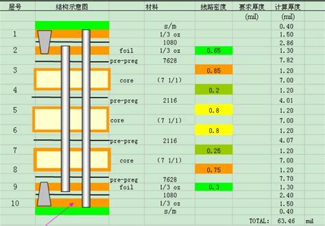
A critical factor in reducing PCB manufacturing cost while maintaining reliability lies in optimizing layer stack-ups and via structures. For instance, using microvias instead of traditional through-holes can improve signal paths and reduce heat buildup—a common failure point in HPC environments. Rigorous testing protocols, such as automated optical inspection (AOI) and thermal cycling, ensure defects are identified before deployment.
For PCB manufacturing businesses serving cloud infrastructure, balancing performance with scalability is key. Proprietary methodologies like embedded trace substrates (ETS) or hybrid rigid-flex designs enable higher component density without compromising durability. By partnering with experienced PCB manufacturing providers, you gain access to failure mode analysis and predictive maintenance models, which extend the lifecycle of mission-critical systems.
Transitioning to next-gen architectures? Focus on how PCB manufacturing processes integrate with cooling solutions and power delivery networks. Even minor inefficiencies in these areas can cascade into reliability issues under sustained computational loads. The right design-for-manufacturing (DFM) strategies ensure your boards withstand the demands of AI workloads, data centers, and beyond.
Flextronics Rigorous Testing Methodologies
To ensure reliability in advanced PCB manufacturing, Flextronics implements multi-layered testing protocols designed to identify and eliminate defects at every production stage. By combining automated optical inspection (AOI) with in-circuit testing (ICT), they validate electrical performance and structural integrity, even in high-density designs. This approach minimizes PCB manufacturing cost risks by catching flaws early, preventing costly rework or field failures.
For PCB manufacturing companies, balancing speed and precision is critical. Flextronics achieves this through real-time data analytics, which optimizes test parameters based on historical performance trends. Their proprietary thermal cycling tests simulate extreme operating conditions, ensuring boards withstand stresses common in cloud infrastructure or high-performance computing environments.
What sets their PCB manufacturing business apart is the integration of AI-driven anomaly detection. Machine learning algorithms analyze thousands of test points, flagging subtle deviations invisible to conventional methods. This proactive strategy not only meets but often exceeds industry standards like IPC-A-610G, reinforcing trust in mission-critical applications. By prioritizing traceability and repeatability, Flextronics ensures each batch maintains consistent quality—a non-negotiable requirement for sectors where downtime translates to significant revenue loss.
Cloud Infrastructure PCB Manufacturing Solutions
When selecting PCB manufacturing companies for cloud infrastructure applications, you need solutions that balance scalability with uncompromising reliability. Flextronics addresses this by integrating PCB manufacturing processes tailored for high-density server architectures, where thermal management and signal integrity are non-negotiable. Their proprietary stack-up designs minimize PCB manufacturing cost through material optimization while ensuring 20% better heat dissipation compared to conventional methods—a critical factor for data centers operating at peak loads.
By leveraging automated optical inspection (AOI) and AI-driven defect detection, Flextronics reduces assembly errors by up to 35%, aligning with the rigorous demands of hyperscale cloud providers. This precision is further enhanced by partnerships with substrate suppliers, ensuring traceability across the PCB manufacturing business chain—from raw materials to final validation. For example, their copper-filled microvia technology supports 40-layer boards without sacrificing impedance control, enabling faster data transmission in next-gen server platforms.
These innovations not only streamline production but also future-proof your infrastructure investments, ensuring compatibility with evolving standards like PCIe 6.0 and DDR5. Whether deploying edge computing nodes or centralized cloud servers, the focus remains on delivering end-to-end reliability without inflating operational overhead—a strategic advantage in competitive PCB manufacturing markets.
Advanced Flextronics PCB Process Innovations
When optimizing PCB manufacturing for cutting-edge applications, process innovation becomes critical to balancing performance and reliability. Flextronics integrates proprietary technologies like laser-direct imaging (LDI) and automated optical inspection (AOI) to refine trace geometries and minimize micro-defects in high-density interconnects. These advancements enable PCB manufacturing companies to address challenges in thermal management and signal integrity, particularly for cloud infrastructure systems requiring sub-6μm line widths.
A key differentiator lies in Flextronics’ adaptive manufacturing workflows, which dynamically adjust parameters like lamination pressure and solder paste deposition. This reduces PCB manufacturing cost by minimizing material waste and rework rates—factors that often escalate expenses in traditional assembly lines. By coupling these processes with AI-driven predictive analytics, you gain real-time insights into potential failure modes, ensuring consistent quality even for complex designs.
For businesses scaling their PCB manufacturing business, Flextronics’ approach offers a strategic edge. Their multi-stage validation protocols—including thermal cycling and impedance testing—ensure boards withstand extreme operational stresses. This focus on precision not only aligns with high-performance computing demands but also future-proofs designs as component miniaturization accelerates. By prioritizing both innovation and scalability, Flextronics bridges the gap between advanced engineering and cost-effective production.
Flextronics PCB for High-Density Applications
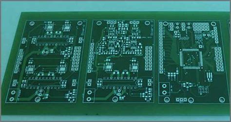
When designing systems requiring high-density interconnects, you need PCB manufacturing solutions that balance miniaturization with electrical integrity. Flextronics addresses this challenge through specialized processes tailored for complex layouts, such as stacked microvias and ultra-fine pitch components. Their approach reduces PCB manufacturing cost by minimizing material waste while maintaining signal integrity—critical for applications like AI accelerators or edge computing devices.
Leading PCB manufacturing companies prioritize thermal management in dense designs, and Flextronics integrates advanced substrates with low-loss dielectrics to dissipate heat efficiently. This ensures reliability even when components are spaced below 0.4mm. For businesses scaling their PCB manufacturing business, Flextronics’ proprietary design-for-manufacturability (DFM) tools streamline prototyping, reducing iteration cycles by up to 30%. By combining laser-drilled apertures with automated optical inspection (AOI), they mitigate risks like solder bridging—a common pain point in high-density assemblies.
Whether you’re developing 5G infrastructure or medical imaging systems, Flextronics’ expertise in high-density PCB manufacturing ensures your designs meet performance benchmarks without compromising scalability.
Ensuring Precision in Flextronics PCB Assembly
Achieving precision in PCB manufacturing requires balancing advanced technologies with meticulous process controls. Flextronics integrates automated optical inspection (AOI) systems and design-for-manufacturability (DFM) principles to minimize deviations during assembly. For high-density applications, even micron-level misalignments can compromise performance, which is why PCB manufacturing companies like Flextronics deploy laser-drilled microvias and precision solder paste printing to ensure component placement accuracy.
To address PCB manufacturing cost challenges without sacrificing quality, their processes leverage predictive analytics to optimize material usage and reduce rework. Rigorous in-line testing, including X-ray inspection and thermal cycling, validates signal integrity and solder joint reliability—critical for high-performance computing environments. This approach not only streamlines the PCB manufacturing business but also aligns with the scalability demands of cloud infrastructure deployments. By combining proprietary defect-prevention protocols with real-time process adjustments, Flextronics ensures that every layer, from substrate lamination to final surface finishing, meets exacting tolerances. Such precision enables consistent performance in applications where power density, thermal management, and signal speed are non-negotiable.
Conclusion
When evaluating reliability in advanced PCB manufacturing, it becomes clear that companies like Flextronics prioritize precision through methodologies tailored for high-performance systems. By integrating proprietary defect-prevention protocols and rigorous testing frameworks, they address critical challenges in PCB manufacturing cost while maintaining compliance with cloud infrastructure demands. For PCB manufacturing companies, this balance between quality and efficiency ensures scalable solutions, particularly for high-density applications requiring flawless signal integrity.
Your decision to partner with established PCB manufacturing business providers hinges on their ability to optimize processes without compromising on traceability or thermal management. Flextronics’ innovations in material selection and automated inspection highlight how advanced assembly techniques mitigate risks inherent to complex designs. Whether deploying systems for high-performance computing or cloud infrastructure applications, aligning with manufacturers that emphasize end-to-end process control ensures long-term reliability—proving that strategic investments in PCB manufacturing ultimately translate to reduced lifecycle costs and enhanced operational trust.
FAQs
How does Flextronics ensure defect prevention in PCB manufacturing?
Flextronics employs proprietary processes, including automated optical inspection (AOI) and real-time thermal profiling, to identify potential defects during assembly. By integrating machine learning algorithms, they reduce errors in high-density applications, ensuring reliability for cloud infrastructure and computing systems.
What factors influence PCB manufacturing costs for advanced assemblies?
Costs depend on material selection, layer count, and testing rigor. Flextronics optimizes PCB manufacturing expenses through design-for-manufacturability (DFM) analysis, minimizing waste while maintaining performance. Their partnerships with leading PCB manufacturing companies also secure competitive material pricing.
Why choose Flextronics for high-performance computing PCB solutions?
Their rigorous testing methodologies, such as accelerated life testing and signal integrity validation, ensure boards withstand extreme workloads. This is critical for data centers and AI-driven systems, where PCB reliability directly impacts operational uptime.
Can Flextronics handle custom PCB manufacturing business requirements?
Yes. Their flexible production lines support low-to-high-volume orders, with rapid prototyping for iterative designs. This scalability makes them ideal for startups and enterprises alike, particularly in evolving sectors like 5G and edge computing.
How do advanced processes improve PCB manufacturing for cloud infrastructure?
Flextronics uses embedded component technology and ultra-fine pitch soldering to enhance signal speed and reduce latency. These innovations address the growing demand for energy-efficient, high-speed interconnects in hyperscale data centers.
Need Expert PCB Manufacturing Services?
For tailored solutions that balance PCB manufacturing cost and performance, please click here to explore how industry-leading practices can elevate your project’s reliability.