FPGA Programming: An In-Depth Exploration
Introduction
Field-Programmable Gate Arrays (FPGAs) have become a cornerstone in modern digital design, offering a unique blend of flexibility, performance, and power efficiency. Unlike traditional processors, which execute instructions sequentially, FPGAs allow for the creation of custom hardware circuits that can perform multiple operations in parallel. This capability makes FPGAs particularly well-suited for applications requiring high-speed data processing, such as telecommunications, automotive systems, and machine learning.
This article delves into the intricacies of FPGA programming, covering the fundamental concepts, design methodologies, tools, and applications. By the end of this exploration, readers will have a comprehensive understanding of how to program FPGAs and the potential they hold in various industries.
Understanding FPGAs
What is an FPGA?
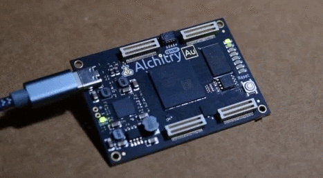
An FPGA is a semiconductor device that can be programmed to perform specific functions by configuring its logic blocks and interconnects. Unlike Application-Specific Integrated Circuits (ASICs), which are custom-designed for a particular application and cannot be altered after fabrication, FPGAs can be reprogrammed multiple times, making them highly versatile.
FPGA Architecture
The architecture of an FPGA consists of three main components:
- Configurable Logic Blocks (CLBs): These are the basic building blocks of an FPGA, containing look-up tables (LUTs), flip-flops, and multiplexers. CLBs can be programmed to implement various logic functions.
- Programmable Interconnects: These are the pathways that connect the CLBs, allowing data to flow between them. The interconnects can be configured to create the desired circuit topology.
- Input/Output Blocks (IOBs): These blocks interface the FPGA with external devices, allowing data to be input to and output from the FPGA.
FPGA vs. Microprocessors
While microprocessors execute instructions sequentially, FPGAs can perform multiple operations simultaneously due to their parallel architecture. This parallelism allows FPGAs to achieve higher performance for certain tasks, such as digital signal processing (DSP) and real-time data analysis. However, FPGAs are generally more complex to program and require a different design approach compared to traditional software development.

FPGA Programming Fundamentals
Hardware Description Languages (HDLs)
FPGA programming is primarily done using Hardware Description Languages (HDLs), with the two most common being VHDL (VHSIC Hardware Description Language) and Verilog. These languages allow designers to describe the behavior and structure of digital circuits at various levels of abstraction.
VHDL
VHDL is a strongly typed language that is often used in academic and European industries. It provides a high level of abstraction, allowing designers to describe complex systems with ease. VHDL is known for its rigorous syntax and strong type checking, which can help prevent errors during the design process.
Verilog
Verilog is more widely used in the United States and Asia. It has a simpler syntax compared to VHDL, making it easier to learn and use. Verilog is often preferred for its brevity and flexibility, especially in large-scale designs.
Design Flow
The FPGA design flow involves several stages, from conceptualization to the final implementation on the device. The typical design flow includes the following steps:
- Specification: Define the requirements and functionality of the design.
- Design Entry: Create the design using HDLs or schematic entry tools.
- Simulation: Verify the design’s functionality using simulation tools to ensure it behaves as expected.
- Synthesis: Convert the HDL code into a netlist, which represents the design in terms of logic gates and interconnects.
- Place and Route: Map the netlist onto the FPGA’s physical resources, determining the placement of logic blocks and the routing of interconnects.
- Bitstream Generation: Generate the configuration file (bitstream) that will be loaded onto the FPGA to program it.
- Configuration: Load the bitstream onto the FPGA to configure it with the desired functionality.
- Testing and Validation: Test the programmed FPGA in the target environment to ensure it meets the design specifications.
Simulation and Verification
Simulation is a critical step in the FPGA design process, allowing designers to test their designs before committing them to hardware. Simulation tools, such as ModelSim and Xilinx Vivado, enable designers to create test benches that simulate the behavior of the design under various conditions. This helps identify and correct errors early in the design process, reducing the risk of costly mistakes during implementation.

Synthesis and Optimization
Synthesis is the process of converting the HDL code into a netlist that can be mapped onto the FPGA’s physical resources. During synthesis, the design is optimized for performance, area, and power consumption. Optimization techniques include logic minimization, resource sharing, and pipelining. The goal is to achieve the best possible performance while minimizing the use of FPGA resources.
Place and Route
The place and route process involves mapping the synthesized netlist onto the FPGA’s physical resources. This includes placing the logic blocks in specific locations on the FPGA and routing the interconnects between them. The quality of the place and route process can significantly impact the performance and reliability of the design. Tools like Xilinx Vivado and Intel Quartus provide automated place and route algorithms, but designers can also manually optimize the placement and routing for critical paths.
Bitstream Generation and Configuration
Once the design has been placed and routed, the next step is to generate the bitstream, which is the binary file used to configure the FPGA. The bitstream contains all the information needed to program the FPGA’s logic blocks and interconnects. The bitstream is then loaded onto the FPGA using a configuration interface, such as JTAG (Joint Test Action Group) or a dedicated configuration memory.
Advanced FPGA Programming Techniques
High-Level Synthesis (HLS)
High-Level Synthesis (HLS) is an advanced technique that allows designers to describe their designs using high-level programming languages like C, C++, or SystemC, rather than traditional HDLs. HLS tools, such as Xilinx Vivado HLS and Intel HLS Compiler, automatically convert the high-level code into HDL, which can then be synthesized and implemented on the FPGA. HLS can significantly reduce development time and make FPGA programming more accessible to software engineers.
Partial Reconfiguration
Partial reconfiguration is a technique that allows specific portions of an FPGA to be reconfigured while the rest of the device continues to operate. This is particularly useful in applications where the FPGA needs to support multiple functions or adapt to changing requirements without interrupting the overall system operation. Partial reconfiguration can be achieved using tools like Xilinx Vivado and Intel Quartus, which support dynamic reconfiguration of FPGA resources.
System-on-Chip (SoC) FPGAs
System-on-Chip (SoC) FPGAs integrate a processor (such as an ARM Cortex-A or Cortex-R) with FPGA fabric on a single chip. This combination allows designers to leverage the flexibility of FPGAs while also benefiting from the ease of software development on a traditional processor. SoC FPGAs are commonly used in applications that require both high-performance processing and custom hardware acceleration, such as embedded vision, automotive systems, and IoT devices.
FPGA-Based DSP and Machine Learning
FPGAs are increasingly being used for digital signal processing (DSP) and machine learning applications due to their ability to perform parallel computations. In DSP, FPGAs can be used to implement filters, Fast Fourier Transforms (FFTs), and other signal processing algorithms with high throughput and low latency. In machine learning, FPGAs can accelerate the training and inference of neural networks by implementing custom hardware architectures optimized for specific algorithms.

FPGA Programming Tools and Ecosystems
Xilinx Vivado
Xilinx Vivado is one of the most popular FPGA design tools, offering a comprehensive suite of features for design entry, synthesis, simulation, place and route, and bitstream generation. Vivado supports both VHDL and Verilog, as well as high-level synthesis using C/C++. It also includes advanced features like partial reconfiguration and system-level design for SoC FPGAs.
Intel Quartus
Intel Quartus is another leading FPGA design tool, providing a similar set of features to Xilinx Vivado. Quartus supports a wide range of Intel FPGAs, including the Stratix, Arria, and Cyclone families. It also offers high-level synthesis, partial reconfiguration, and support for SoC FPGAs with integrated ARM processors.
Open-Source Tools
In addition to commercial tools, there are several open-source tools available for FPGA programming. These include:
- Yosys: An open-source synthesis tool that supports Verilog and can be used to generate netlists for various FPGA architectures.
- Nextpnr: An open-source place and route tool that works with Yosys and supports multiple FPGA families, including Lattice iCE40 and ECP5.
- Verilator: An open-source tool for simulating Verilog designs, offering high performance and flexibility.
Open-source tools are particularly appealing for hobbyists and researchers who want to experiment with FPGA programming without the cost of commercial software.
Applications of FPGA Programming
Telecommunications
FPGAs are widely used in telecommunications for tasks such as signal processing, error correction, and protocol handling. Their ability to process data in parallel makes them ideal for high-speed communication systems, including 5G networks and optical communication.
Automotive
In the automotive industry, FPGAs are used for advanced driver-assistance systems (ADAS), infotainment systems, and engine control units (ECUs). FPGAs can process sensor data in real-time, enabling features like lane departure warning, adaptive cruise control, and autonomous driving.
Aerospace and Defense
FPGAs are critical in aerospace and defense applications, where they are used for radar systems, electronic warfare, and secure communications. Their reprogrammability allows for rapid updates and adaptations to changing mission requirements.
Medical Imaging
In medical imaging, FPGAs are used to process data from devices like MRI machines, CT scanners, and ultrasound systems. Their parallel processing capabilities enable real-time image reconstruction and analysis, improving diagnostic accuracy and patient outcomes.
Machine Learning and AI
FPGAs are increasingly being used to accelerate machine learning and AI workloads. Their ability to perform parallel computations makes them well-suited for tasks like neural network inference, where low latency and high throughput are critical.
Conclusion
FPGA programming is a powerful and versatile skill that opens up a world of possibilities in digital design. From telecommunications to machine learning, FPGAs are transforming industries by enabling high-performance, customizable hardware solutions. While FPGA programming can be complex, the availability of advanced tools and techniques, such as high-level synthesis and partial reconfiguration, is making it more accessible than ever.
As technology continues to evolve, the role of FPGAs is likely to expand, driven by the growing demand for parallel processing and hardware acceleration. Whether you’re a seasoned engineer or a curious hobbyist, learning FPGA programming is a valuable investment in the future of digital design.


