Fr4 circuit board manufacturing
Understanding The Basics Of FR4 Circuit Board Manufacturing
FR4 circuit board manufacturing is a fundamental process in the electronics industry, serving as the backbone for a wide array of electronic devices. Understanding the basics of this manufacturing process is crucial for anyone involved in electronics design and production.
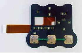
At the core of this process is the FR4 material, a composite made from woven fiberglass cloth with an epoxy resin binder that is flame resistant.
This material is renowned for its excellent strength-to-weight ratio, electrical insulation properties, and resistance to moisture, making it an ideal substrate for printed circuit boards (PCBs).
The manufacturing process begins with the selection of the appropriate FR4 laminate, which is available in various thicknesses and copper cladding options.
The choice of laminate depends on the specific requirements of the electronic device, such as its operating environment and electrical performance needs. Once the laminate is selected, the next step involves designing the circuit layout. This is typically done using computer-aided design (CAD) software, which allows engineers to create precise and intricate circuit patterns.
Following the design phase, the manufacturing process moves to the fabrication stage, where the circuit pattern is transferred onto the FR4 substrate.
This is achieved through a process known as photolithography. In this process, a photosensitive film is applied to the copper-clad FR4 board, and the circuit pattern is projected onto the film using ultraviolet light. The exposed areas of the film are then developed, revealing the copper that needs to be etched away. The etching process removes the unwanted copper, leaving behind the desired circuit pattern.
Once the etching is complete, the next step is drilling.
This involves creating holes in the board for component leads and vias, which are used to connect different layers of the board. Precision drilling is essential to ensure that the holes are accurately placed and sized, as any deviation can affect the board’s performance. After drilling, the board undergoes a plating process, where a thin layer of copper is deposited onto the walls of the drilled holes. This step is crucial for establishing electrical connections between the different layers of the board.
Subsequently, the board is subjected to a solder mask application.
The solder mask is a protective layer that prevents solder bridges from forming between closely spaced components during assembly. It also provides a degree of protection against environmental factors such as moisture and dust. The application of the solder mask is followed by the silkscreen process, where component labels and other markings are printed onto the board for easy identification during assembly.
Finally, the board undergoes a series of inspections and tests to ensure its quality and functionality.
These tests may include electrical testing to verify the integrity of the circuit connections and visual inspections to check for any physical defects. Once the board passes these tests, it is ready for assembly, where electronic components are mounted onto the board to create a functional electronic device.
In conclusion, FR4 circuit board manufacturing is a complex process that requires careful attention to detail at every stage. From selecting the right materials to ensuring precise fabrication and assembly, each step is critical to producing high-quality PCBs that meet the demands of modern electronic applications. Understanding these basics provides valuable insight into the intricate world of electronics manufacturing.
Key Steps In The FR4 PCB Production Process
The production of FR4 circuit boards, a staple in the electronics industry, involves a series of meticulously coordinated steps that ensure the final product meets the required specifications and quality standards. FR4, a composite material made from woven fiberglass cloth with an epoxy resin binder, is renowned for its excellent strength-to-weight ratio and electrical insulation properties. Understanding the key steps in the FR4 PCB production process is essential for appreciating the complexity and precision involved in manufacturing these critical components.
The process begins with the design phase, where engineers use specialized software to create detailed schematics and layouts of the circuit board.
This step is crucial as it determines the functionality and performance of the final product. Once the design is finalized, it is converted into a format suitable for manufacturing, typically a Gerber file, which contains all the necessary information about the board’s layers, traces, and components.
Following the design phase, the next step is the preparation of the FR4 substrate.
This involves cutting the FR4 sheets to the required size and cleaning them to remove any contaminants that could affect the adhesion of subsequent layers. The cleaned substrate is then laminated with a layer of copper foil on one or both sides, depending on whether a single or double-sided PCB is being produced. This copper layer will form the conductive pathways of the circuit.
The subsequent step is the application of a photosensitive resist to the copper-clad substrate.
This resist is essential for the photolithography process, where the board is exposed to ultraviolet light through a photomask that corresponds to the circuit design. The areas exposed to the light harden, while the unexposed areas remain soft and are subsequently washed away, revealing the copper beneath.
Etching follows, where the exposed copper is removed using a chemical solution, leaving behind only the desired copper traces that form the circuit. After etching, the remaining photoresist is stripped away, and the board undergoes a thorough cleaning to ensure no residues remain.
Drilling is the next critical step, where holes are drilled into the board to accommodate component leads and vias,
which are essential for electrical connections between different layers of the board. Precision is paramount in this step, as any misalignment can lead to faulty connections and compromised board functionality.
Once drilling is complete, the board undergoes a plating process to deposit a thin layer of copper into the drilled holes
ensuring electrical connectivity. This is followed by the application of a solder mask, which is a protective layer that prevents solder from bridging between conductive traces and protects the board from environmental damage.
The final steps in the FR4 PCB production process include the application of a silkscreen layer
which provides component labels and other important information, and the surface finish, which enhances solderability and protects the exposed copper. The boards are then subjected to rigorous testing to verify their electrical performance and adherence to design specifications.
In conclusion, the production of FR4 circuit boards is a complex process that requires precision and attention to detail at every stage. From design to final testing, each step is crucial in ensuring that the final product meets the high standards required for modern electronic devices. Understanding these key steps provides valuable insight into the intricate world of PCB manufacturing.
Advantages Of Using FR4 Material In Circuit Boards
FR4 material has become a cornerstone in the manufacturing of circuit boards, primarily due to its exceptional properties that cater to the demanding needs of modern electronics. As the backbone of printed circuit boards (PCBs), FR4 offers a multitude of advantages that make it the preferred choice for engineers and manufacturers alike. Understanding these benefits is crucial for appreciating why FR4 remains a dominant material in the electronics industry.
To begin with, one of the most significant advantages of FR4 material is its excellent electrical insulation properties.
This characteristic is vital for ensuring that the circuit board can effectively manage electrical currents without risk of short circuits or electrical failures. The material’s ability to maintain its insulating properties even under high temperatures further enhances its reliability, making it suitable for a wide range of applications, from consumer electronics to industrial machinery.
In addition to its insulating capabilities, FR4 is renowned for its mechanical strength.
The material is composed of woven fiberglass cloth with an epoxy resin binder, which provides a robust and durable structure. This strength is essential for supporting the various components mounted on the circuit board, ensuring that they remain securely in place even under mechanical stress or vibration. Consequently, FR4 circuit boards are less prone to damage during manufacturing, transportation, and operation, which translates to longer-lasting and more reliable electronic devices.
Moreover, FR4 material exhibits excellent thermal resistance, a critical factor in the performance and longevity of electronic devices.
As electronic components generate heat during operation, the ability of the circuit board to withstand and dissipate this heat is crucial. FR4’s thermal stability ensures that it can operate effectively in environments with fluctuating temperatures, reducing the risk of thermal-related failures. This property is particularly beneficial in applications where devices are exposed to harsh conditions, such as automotive or aerospace industries.
Furthermore, the cost-effectiveness of FR4 material cannot be overlooked.
Compared to other high-performance materials, FR4 offers a balance between performance and affordability, making it an attractive option for manufacturers looking to optimize production costs without compromising quality. Its widespread availability and ease of processing also contribute to its cost advantages, allowing for efficient manufacturing processes and quick turnaround times.
Another noteworthy advantage of FR4 is its versatility.
The material can be easily modified to meet specific requirements, such as varying thicknesses or different surface finishes, to suit diverse applications. This adaptability makes FR4 suitable for a wide range of electronic products, from simple consumer gadgets to complex industrial systems. Additionally, FR4’s compatibility with various fabrication techniques, such as multilayer construction, further expands its application potential, enabling the development of sophisticated and compact electronic devices.
In conclusion, the advantages of using FR4 material in circuit board manufacturing are manifold. Its excellent electrical insulation, mechanical strength, thermal resistance, cost-effectiveness, and versatility make it an ideal choice for a broad spectrum of electronic applications. As technology continues to advance, the demand for reliable and efficient circuit boards will only grow, and FR4 is well-positioned to meet these evolving needs. By leveraging the unique properties of FR4, manufacturers can ensure the production of high-quality circuit boards that meet the rigorous demands of modern electronics.
Common Challenges In FR4 Circuit Board Manufacturing And Solutions
FR4 circuit board manufacturing is a critical process in the electronics industry, serving as the backbone for a wide array of electronic devices. However, this process is not without its challenges. Understanding these challenges and implementing effective solutions is essential for manufacturers aiming to produce high-quality circuit boards efficiently.
One of the primary challenges in FR4 circuit board manufacturing is maintaining the integrity of the material during the fabrication process.
FR4, a composite material made of woven fiberglass cloth with an epoxy resin binder, is valued for its excellent mechanical strength and electrical insulation properties. However, its sensitivity to temperature and moisture can lead to warping or delamination if not properly managed. To address this, manufacturers must ensure precise control of environmental conditions throughout the production process. Implementing advanced climate control systems in manufacturing facilities can help maintain optimal temperature and humidity levels, thereby reducing the risk of material degradation.
Another significant challenge is achieving precise layer alignment during the multilayer board fabrication.
Misalignment can lead to electrical failures and reduced performance of the final product. To mitigate this issue, manufacturers can employ automated optical inspection systems that provide real-time feedback and ensure accurate layer registration. Additionally, investing in high-precision drilling and imaging equipment can further enhance alignment accuracy, minimizing the potential for defects.
The etching process, which involves removing excess copper to create the desired circuit patterns, also presents challenges.
Inconsistent etching can result in incomplete or over-etched circuits, leading to functional failures. To overcome this, manufacturers can adopt advanced etching techniques such as laser etching, which offers greater precision and control compared to traditional chemical methods. Furthermore, regular calibration and maintenance of etching equipment are crucial to ensure consistent performance and high-quality output.
Solder mask application is another area where challenges frequently arise.
The solder mask, a protective layer applied to prevent solder bridges and corrosion, must be applied uniformly to avoid defects. Variations in solder mask thickness can lead to issues such as poor adhesion or insufficient coverage. To address this, manufacturers can utilize automated solder mask application systems that ensure consistent thickness and coverage across the entire board. Additionally, implementing rigorous quality control measures, such as visual inspections and thickness measurements, can help identify and rectify any inconsistencies early in the process.
Moreover, the increasing complexity of circuit board designs poses a challenge in terms of testing and quality assurance.
As boards become more intricate, with higher component densities and smaller traces, traditional testing methods may prove inadequate. To tackle this, manufacturers can employ advanced testing technologies such as automated optical inspection (AOI) and X-ray inspection, which provide detailed insights into the board’s structural and electrical integrity. These technologies enable the detection of defects that may not be visible to the naked eye, ensuring that only boards meeting stringent quality standards proceed to the next stage of production.
In conclusion, while FR4 circuit board manufacturing presents several challenges, adopting innovative solutions and technologies can significantly enhance the quality and efficiency of the production process. By addressing issues related to material integrity, layer alignment, etching precision, solder mask application, and testing, manufacturers can overcome these challenges and deliver reliable, high-performance circuit boards to meet the demands of the ever-evolving electronics industry.