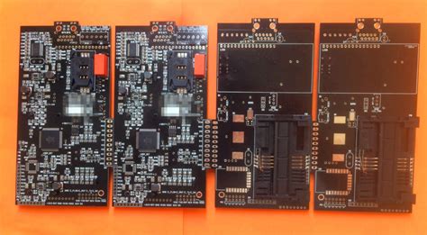
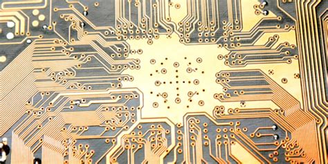
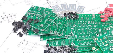
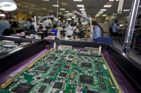
Frequently Asked Questions about PCB Design (I)
1.How to choose PCB material?
The selection of PCB material must strike a balance between meeting design requirements and mass production and cost. Design requirements include electrical and mechanical parts. Usually, this material issue is more important when designing very high-speed PCB boards (frequencies greater than GHz). For example, the dielectric loss of the commonly used FR-4 material at frequencies of several GHz will have a great impact on signal attenuation and may not be suitable. In terms of electrical, it is necessary to pay attention to whether the dielectric constant and dielectric loss are suitable for the designed frequency.
2.How to avoid high-frequency interference?
The basic idea of avoiding high-frequency interference is to minimize the interference of the electromagnetic field of high-frequency signals, which is also called crosstalk. You can increase the distance between high-speed signals and analog signals, or add ground guard/shunt traces next to analog signals. Also pay attention to the noise interference of digital ground to analog ground.
3.In high-speed design, how to solve the signal integrity problem?
Signal integrity is basically an impedance matching problem. The factors that affect impedance matching include the architecture and output impedance of the signal source, the characteristic impedance of the trace, the characteristics of the load end, the topology of the trace, etc. The solution is to rely on termination and adjust the topology of the trace.
4.How is the differential wiring method implemented?
There are two points to note when wiring differential pairs. One is that the lengths of the two lines should be as equal as possible, and the other is that the spacing between the two lines (this spacing is determined by the differential impedance) should remain unchanged, that is, they should remain parallel. There are two parallel methods, one is that the two lines run on the same routing layer (side-by-side), and the other is that the two lines run on the upper and lower adjacent layers (over-under). Generally, the former side-by-side is implemented more.
5.For clock signal lines with only one output end, how to implement differential wiring?
To use differential wiring, it must be that the signal source and the receiving end are also differential signals. Therefore, differential wiring cannot be used for clock signals with only one output end.
6.Can a matching resistor be added between the differential line pairs at the receiving end?
Matching resistors are usually added between differential pairs at the receiving end, and their values should be equal to the value of differential impedance. This will improve the signal quality.
7.Why should the wiring of differential pairs be close and parallel?
The wiring of differential pairs should be appropriately close and parallel. The so-called appropriate closeness is because this spacing will affect the value of differential impedance, which is an important parameter for designing differential pairs. Parallel is also required because the consistency of differential impedance must be maintained. If the two lines are sometimes far and sometimes close, the differential impedance will be inconsistent, which will affect the signal integrity and timing delay.
8.How to deal with some theoretical conflicts in actual wiring
1). Basically, it is right to separate and isolate analog/digital grounds. It should be noted that the signal routing should try not to cross the split place (moat), and the returning current path of the power supply and signal should not be too large.
2). The crystal oscillator is an analog positive feedback oscillation circuit. To have a stable oscillation signal, the loop gain and phase specifications must be met. However, the oscillation specifications of this analog signal are easily disturbed. Even if ground guard traces are added, it may not be possible to completely isolate the interference. Moreover, if they are too far away, the noise on the ground plane will also affect the positive feedback oscillation circuit. Therefore, the distance between the crystal oscillator and the chip must be as close as possible.
3). It is true that there are many conflicts between high-speed wiring and EMI requirements. But the basic principle is that the resistors, capacitors or ferrite beads added due to EMI cannot cause some electrical characteristics of the signal to be inconsistent with the specifications. Therefore, it is best to use the techniques of arranging routing and PCB stacking to solve or reduce EMI problems, such as routing high-speed signals on the inner layer. Finally, use resistors, capacitors or ferrite beads to reduce damage to the signal.
9.How to solve the contradiction between manual wiring and automatic wiring of high-speed signals?
Most of the automatic wiring machines of the current stronger wiring software have set constraints to control the winding method and the number of vias. The winding engine capabilities and constraint setting items of various EDA companies are sometimes far apart. For example, whether there are enough constraints to control the winding mode of the serpentine, whether the spacing of the differential pair can be controlled, etc. This will affect whether the routing mode of the automatic routing can meet the designer’s ideas. In addition, the difficulty of manually adjusting the routing is absolutely related to the ability of the winding engine. For example, the pushing ability of the routing, the pushing ability of the via, and even the pushing ability of the routing pair copper, etc. Therefore, choosing a routing device with a strong winding engine is the solution.
10.About test coupons.
The test coupon is used to measure the characteristic impedance of the produced PCB board with TDR (Time Domain Reflectometer) to see if it meets the design requirements. Generally, the impedance to be controlled is single line and differential pair. Therefore, the line width and line spacing (when there is a differential pair) on the test coupon should be the same as the line to be controlled. The most important thing is the position of the ground point during measurement. In order to reduce the inductance of the ground lead, the grounding point of the TDR probe is usually very close to the probe tip. Therefore, the distance and method between the signal measurement point and the grounding point on the test coupon should be consistent with the probe used.
11.In high-speed PCB design, the blank area of the signal layer can be
copper-plated, and how should the copper of multiple signal layers be distributed on the ground and power supply?
Generally, the copper in the blank area is grounded in most cases. However, when copper is applied next to the high-speed signal line, attention should be paid to the distance between the copper and the signal line, because the copper applied will reduce the characteristic impedance of the trace. Also, be careful not to affect the characteristic impedance of other layers, such as in the dual stripline structure.
12.Can the characteristic impedance of the signal line on the power plane be calculated using the microstrip line model? Can the signal between the power and ground planes be calculated using the stripline model?
Yes, both the power plane and the ground plane must be considered as reference planes when calculating the characteristic impedance. For example, a four-layer board: top layer-power layer-ground layer-bottom layer. At this time, the model of the characteristic impedance of the top layer routing is a microstrip line model with the power plane as the reference plane.
13.Can the automatic generation of test points by software on high-density printed circuit boards generally meet the test requirements of mass production?
Whether the test points automatically generated by general software meet the test requirements must be determined by whether the specifications for adding test points meet the requirements of the test equipment. In addition, if the routing is too dense and the specifications for adding test points are strict, it may not be possible to automatically add test points to each line. Of course, you need to manually fill in the places to be tested.
14.Will adding test points affect the quality of high-speed signals?
As for whether it will affect the signal quality, it depends on the way of adding test points and how fast the signal is. Basically, the additional test points (not using the existing perforations (via or DIP pin) on the line as test points) may be added to the line or a small line may be pulled out from the line. The former is equivalent to adding a very small capacitor on the line, and the latter is an additional branch. Both of these situations will have some impact on high-speed signals, and the extent of the impact is related to the frequency speed of the signal and the edge rate of the signal. The magnitude of the impact can be learned through simulation. In principle, the smaller the test point, the better (of course, it must meet the requirements of the test equipment) and the shorter the branch, the better.
15.How should the ground wires between the boards of a system be connected?
When the signals or power supplies between the interconnected PCB boards are in operation, for example, when the power supply or signal of board A is sent to board B, there must be an equal amount of current flowing back from the ground layer to board A (this is Kirchoff current law). The current on the ground layer will flow back to the place with the lowest impedance. Therefore, at each interface where the power supply or signal is connected to each other, the number of pins allocated to the ground layer cannot be too small to reduce the impedance, which can reduce the noise on the ground layer. In addition, the entire current loop can be analyzed, especially the part with larger current, and the connection method of the ground layer or ground wire can be adjusted to control the flow of current (for example, create low impedance at a certain place to let most of the current flow from this place) to reduce the impact on other more sensitive signals.
16.Two commonly referenced characteristic impedance formulas:
a. Microstrip
Z={87/[sqrt(Er+1.41)]}ln[5.98H/(0.8W+T)] Where W is the line width, T is the copper thickness of the trace, H is the distance from the trace to the reference plane, and Er is the dielectric constant of the PCB material. This formula can only be applied when 0.1<(W/H)<2.0 and 1<(Er)<15.
b. Stripline
Z=[60/sqrt(Er)]ln{4H/[0.67π(T+0.8W)]} Where H is the distance between the two reference planes, and the trace is located in the middle of the two reference planes. This formula can only be applied when W/H<0.35 and T/H<0.25.
17.Can a ground wire be added in the middle of a differential signal line?
Generally, a ground wire cannot be added in the middle of a differential signal. Because the most important point of the application principle of differential signals is to utilize the benefits brought by the mutual coupling (coupling) between differential signals, such as flux cancellation, noise immunity, etc. If a ground wire is added in the middle, the coupling effect will be destroyed.
18.Does the design of rigid-flexible boards require special design software and specifications?
Flexible printed circuits (Flexible Printed Circuit) can be designed with general PCB design software. They are also produced by FPC manufacturers in the Gerber format. Because the manufacturing process is different from that of general PCBs, each manufacturer will have restrictions on the minimum line width, minimum line spacing, and minimum aperture (via) based on their manufacturing capabilities. In addition, some copper foil can be laid at the turning point of the flexible circuit board for reinforcement. The inspection standard for soft boards is usually based on IPC6013
19.What is the principle of appropriately selecting the grounding point of the PCB and the shell?
The principle of selecting the grounding point of the PCB and the shell is to use the chassis ground to provide a low-impedance path for the return current and control the path of this return current. For example, usually near high-frequency devices or clock generators, the ground layer of the PCB can be connected to the chassis ground by fixing screws to minimize the area of the entire current loop, thereby reducing electromagnetic radiation.
20.Which aspects should be considered for circuit board debugging?
For digital circuits, first determine three things in order:
Confirm that the values of all power supplies meet the design requirements. Some systems with multiple power supplies may require certain specifications for the order and speed of certain power supplies.
Confirm that all clock signal frequencies are working properly and there are no non-monotonic problems on the signal edges.
Confirm whether the reset signal meets the specification requirements.
If all these are normal, the chip should send the first cycle signal. Next, debug according to the system operation principle and bus protocol.
21.If the size of the circuit board is fixed, if the design needs to accommodate more functions, it is often necessary to increase the routing density of the PCB.
However, this may lead to increased mutual interference between the routings, and the impedance cannot be reduced if the routing is too thin. Please introduce the techniques in high-speed (>100MHz) high-density PCB design?
When designing high-speed and high-density PCBs, crosstalk interference is indeed something that needs special attention, because it has a great impact on timing and signal integrity.
Here are a few points to note:
1). Control the continuity and matching of the routing characteristic impedance.
2). The size of the routing spacing.
The spacing commonly seen is twice the line width. The impact of routing spacing on timing and signal integrity can be understood through simulation, and the minimum tolerable spacing can be found. The results of different chip signals may be different.
3). Choose the appropriate termination method.
4). Avoid the same routing direction of the upper and lower adjacent layers, or even have the routing overlapped up and down, because this crosstalk is greater than the case of adjacent routing on the same layer.
5). Use blind/buried vias to increase the trace area. However, the production cost of the PCB board will increase.
It is indeed difficult to achieve complete parallelism and equal length in actual implementation, but we should try our best to do so. In addition, differential termination and common mode termination can be reserved to mitigate the impact on timing and signal integrity.
22.LC circuits are often used for filtering at analog power supplies. But why is LC sometimes worse than RC filtering?
The comparison of LC and RC filtering effects must consider whether the frequency band to be filtered out and the selection of inductance value are appropriate. Because the reactance of the inductor is related to the inductance value and frequency. If the noise frequency of the power supply is low and the inductance value is not large enough, the filtering effect may not be as good as RC. However, the price of using RC filtering is that the resistor itself consumes energy and has poor efficiency, and attention should be paid to the power that the selected resistor can withstand.


