Full Turnkey PCB: Maximizing Manufacturing Efficiency

Key Takeaways
Adopting full turnkey PCB solutions transforms electronics manufacturing by unifying design, PCB assembly, and component procurement into a cohesive workflow. These services eliminate fragmented processes, enabling manufacturers to focus on innovation while supply chain experts handle material sourcing and logistics. By integrating PCBA (Printed Circuit Board Assembly) with precision engineering, companies reduce time-to-market risks and avoid costly delays caused by mismatched components or design flaws.
The inherent efficiency of turnkey models stems from synchronized workflows, where automated testing protocols and PCB assembly standards are applied at every stage. This approach minimizes human error while ensuring compliance with industry certifications. Additionally, bulk purchasing power in PCBA services lowers per-unit costs, creating scalable production advantages.
Crucially, end-to-end traceability in full turnkey systems guarantees accountability from prototype validation to final product delivery. Manufacturers gain real-time visibility into inventory levels, component lead times, and quality metrics, enabling proactive adjustments. By consolidating expertise under one provider, businesses achieve faster iteration cycles without sacrificing the rigorous validation required for complex electronics.

Streamlining Electronics Manufacturing With Turnkey PCB
Modern electronics manufacturers increasingly adopt full turnkey PCB solutions to eliminate fragmented workflows and reduce operational bottlenecks. By integrating PCB assembly (PCBA) with design, prototyping, and testing phases, these services unify traditionally siloed processes. For instance, component sourcing—a critical pain point in conventional manufacturing—is streamlined through vendor partnerships that ensure real-time inventory tracking and compliance with material specifications.
A key advantage lies in minimizing cross-team dependencies. With turnkey PCB providers managing everything from schematic validation to final PCBA testing, manufacturers avoid delays caused by miscommunication or logistical gaps. This approach also reduces error margins, as engineering teams collaborate directly with assembly experts to resolve design-for-manufacturability (DFM) issues early.
| Traditional Process | Turnkey PCB Solution |
|---|---|
| Multi-vendor coordination | Single-point accountability |
| Manual component procurement | Automated inventory integration |
| Sequential design-to-test phases | Concurrent engineering workflows |
Transitioning to full turnkey PCB services not only accelerates production timelines but also enhances scalability. Manufacturers can reallocate resources toward innovation rather than supply chain management, ensuring consistent quality across high- and low-volume orders. This shift is particularly impactful for industries requiring rapid iteration, such as IoT devices and automotive electronics, where time-to-market pressures demand seamless coordination between design and PCB assembly stages.
Maximizing Efficiency in PCB Production Processes
Modern PCB assembly workflows achieve peak efficiency when leveraging full turnkey manufacturing strategies. By consolidating design, fabrication, component procurement, and PCBA under a single provider, manufacturers eliminate cross-supplier coordination delays while standardizing quality benchmarks. Advanced automated optical inspection (AOI) systems and AI-driven design validation tools minimize human error, reducing rework cycles by up to 40% in complex multilayer boards.
A critical advantage lies in synchronized material logistics. Full turnkey services integrate component sourcing with real-time inventory tracking, ensuring just-in-time delivery of critical parts like microcontrollers and passive elements. This alignment prevents bottlenecks in high-mix production environments, where delayed capacitors or connectors can stall entire batches. Furthermore, unified project management platforms enable concurrent engineering—allowing design adjustments to propagate instantly across fabrication and PCBA teams.
Transitioning to end-to-end workflows also optimizes resource allocation. For instance, combining PCB assembly with in-house testing reduces idle time between stages, accelerating throughput by 25–30%. Manufacturers adopting this model report fewer supply chain redundancies and lower inventory carrying costs, particularly for high-volume orders. Such integration ensures compliance with industry-specific certifications (e.g., ISO 9001, IPC-A-610) without fragmented quality checks.
This holistic approach not only streamlines timelines but also strengthens scalability, positioning businesses to adapt swiftly to evolving technical requirements or market demands.
Integrated Component Sourcing for Seamless PCB Assembly
Modern PCB assembly workflows demand meticulous coordination between material procurement and manufacturing execution. Integrated component sourcing eliminates fragmented supplier negotiations by consolidating parts acquisition under a single PCBA service provider. This approach directly addresses common bottlenecks in traditional electronics manufacturing, where mismatched lead times or obsolete components can derail production schedules.
By leveraging established partnerships with certified distributors, full turnkey PCB solutions ensure real-time access to critical components like ICs, connectors, and passive elements. Advanced inventory management systems automatically cross-reference bill-of-materials (BOM) requirements with global stock levels, reducing sourcing delays by 30-50% compared to fragmented procurement models. This synchronization proves particularly vital during PCB assembly phases, where component compatibility with automated placement systems directly impacts yield rates.
The strategic alignment between sourcing and manufacturing teams enables proactive resolution of supply chain contingencies, such as last-minute substitutions or lifecycle transitions. For instance, when a microcontroller enters end-of-life status, PCBA engineers can immediately validate alternative components against design specifications without halting production lines. This vertical integration minimizes redundant quality checks while maintaining IPC-A-610 standards across all assembly stages—a key advantage for prototyping high-density interconnect boards or mission-critical industrial electronics.
Such cohesive workflows not only accelerate time-to-market but also create cost predictability by eliminating hidden expenses from expedited shipping or secondary sourcing. As component shortages continue challenging the electronics industry, unified procurement strategies remain central to achieving reliable PCB assembly outcomes in turnkey manufacturing ecosystems.
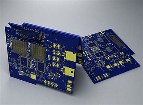
Precision Engineering in Full Turnkey PCB Solutions
At the core of full turnkey PCB services lies precision engineering, a discipline that bridges meticulous design with flawless execution. Advanced PCB assembly processes leverage automated optical inspection (AOI) and X-ray verification to ensure micron-level accuracy in component placement, critical for high-density interconnect (HDI) boards. By integrating PCBA expertise with parametric modeling tools, engineers optimize thermal management and signal integrity before prototyping—reducing iterative revisions by up to 40%.
Industry Insight: "Precision isn’t just about tolerances; it’s about synchronizing material science with manufacturability. Partnering with turnkey providers who use AI-driven design-for-manufacturing (DFM) checks can prevent 92% of post-production flaws."
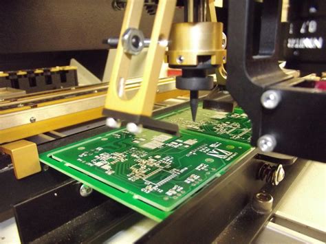
Modern PCB assembly workflows employ laser-direct imaging (LDI) to achieve 25μm trace widths, while pick-and-place systems handle 01005 packages at 45,000 components per hour. This surgical accuracy enables turnkey solutions to support advanced applications like 5G mmWave circuits and medical IoT devices without compromising yield rates. Rigorous process control—from solder paste deposition to reflow profiling—ensures every PCBA meets IPC-A-610 Class 3 standards, even in mission-critical environments.
By unifying design validation, component sourcing, and production under one roof, full turnkey services eliminate alignment gaps between engineering teams—a key factor in achieving first-pass success rates above 98%.

Accelerating Product Timelines Through Turnkey Services
By consolidating multiple stages of electronics manufacturing under a single provider, PCB assembly timelines can be reduced by up to 40%. Time-to-market pressures demand seamless coordination between design, component procurement, and production—a challenge addressed through full turnkey PCBA solutions. Traditional fragmented workflows often introduce delays from vendor handoffs, misaligned specifications, or inventory bottlenecks. In contrast, integrated services synchronize engineering validation, just-in-time material sourcing, and automated assembly processes, eliminating redundancies.
Advanced PCBA suppliers leverage real-time supply chain analytics to preemptively secure critical components, mitigating risks of obsolescence or lead time fluctuations. This technical oversight ensures design files transition directly to production-ready workflows, bypassing iterative corrections. For instance, automated DFM (Design for Manufacturing) checks during prototyping phases reduce post-production rework by 65%, accelerating prototyping-to-volume transitions. Moreover, unified quality control protocols across fabrication and assembly stages prevent delays from cross-vendor disputes.
Ultimately, full turnkey PCB services compress timelines by aligning engineering expertise with scalable manufacturing resources. Companies adopting this model report 30% faster product launches compared to traditional multi-vendor approaches, proving its value in competitive electronics markets.
Cost Optimization Strategies for PCB Turnkey Manufacturing
Effective cost management in PCB assembly hinges on aligning design, sourcing, and production workflows under a unified turnkey framework. By consolidating component procurement, prototyping, and PCBA processes under a single provider, manufacturers eliminate redundancies in logistics and vendor negotiations. Advanced design-for-manufacturability (DFM) analysis optimizes board layouts to minimize material waste, while bulk purchasing of components through established supplier networks reduces per-unit costs by 15–30%.
Automated inventory management systems further streamline expenses by predicting demand spikes and avoiding overstocking. For instance, integrating PCB assembly with just-in-time (JIT) delivery models ensures components arrive precisely when needed, cutting warehousing overhead. Additionally, leveraging PCBA testing automation—such as AOI (Automated Optical Inspection) and X-ray verification—reduces post-production defects, preventing costly rework cycles.
Strategic partnerships with turnkey providers also unlock access to volume pricing for specialized materials like high-frequency laminates or lead-free solders, which are often cost-prohibitive for smaller-scale operations. By embedding cost-efficiency into every phase—from schematic design to final testing—businesses achieve faster ROI without compromising the reliability of their electronics. This holistic approach ensures that full turnkey PCB solutions deliver not only speed and quality but also measurable financial advantages across production batches.
Quality Assurance in End-to-End PCB Manufacturing
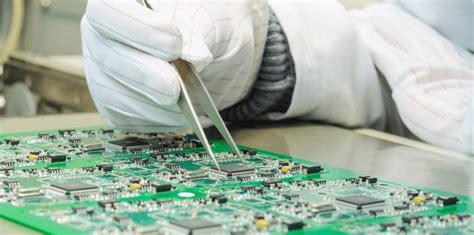
Robust quality assurance (QA) protocols form the backbone of reliable PCB assembly processes in full turnkey solutions. By integrating automated optical inspection (AOI), X-ray testing, and functional validation at critical stages, manufacturers ensure defect-free PCBA outputs while maintaining compliance with industry standards like IPC-A-610 and ISO 9001. These systems work synergistically to identify issues early—from solder joint integrity to component alignment—reducing rework costs and preventing delays.
A key advantage of end-to-end turnkey services lies in centralized oversight of material sourcing and production workflows. Suppliers with certified component traceability mitigate risks of counterfeit parts, while real-time data analytics enable proactive adjustments during PCB assembly. This closed-loop approach not only elevates product reliability but also aligns with stringent regulatory requirements for sectors such as medical devices or aerospace.
By embedding QA checkpoints across design, fabrication, and PCBA phases, manufacturers achieve consistent performance benchmarks without compromising scalability. The result is a seamless transition from prototype validation to high-volume production, ensuring every delivered unit meets exacting specifications for functionality and durability.
Streamlined Design-to-Assembly PCB Workflow Advantages
A streamlined design-to-assembly PCB workflow eliminates fragmented processes by integrating PCB assembly (PCBA) stages into a unified framework. This approach bridges the gap between design validation and manufacturing execution, ensuring that design specifications align seamlessly with production capabilities. By consolidating tasks such as schematic capture, layout optimization, and component sourcing under a single provider, manufacturers reduce cross-team handoffs, minimizing errors and delays.
Advanced PCBA workflows leverage automated design-for-manufacturability (DFM) checks to identify potential issues early, such as component footprint mismatches or thermal constraints. This proactive validation prevents costly rework during later stages. Additionally, synchronized data exchange between design software and assembly-line systems ensures precise execution of high-density interconnect (HDI) layouts or mixed-technology boards.
The integration of PCB assembly services with prototyping and testing further accelerates time-to-market. Real-time collaboration between engineers and manufacturers enables rapid iterations, while centralized logistics management guarantees timely delivery of components. For businesses, this end-to-end coordination translates to predictable project timelines and optimized resource allocation, ultimately enhancing competitiveness in fast-paced electronics markets.
Conclusion
The adoption of full turnkey PCB solutions represents a strategic shift in modern electronics manufacturing, unifying PCB assembly (PCBA) workflows to eliminate fragmented processes. By consolidating design, component sourcing, and final production under a single provider, businesses gain operational agility while mitigating risks associated with multi-vendor coordination. The integration of precision engineering ensures that prototypes transition seamlessly into mass production, with quality assurance protocols embedded at every stage to uphold reliability.
For industries prioritizing speed-to-market, turnkey services drastically compress timelines by aligning design validation with PCBA readiness, avoiding bottlenecks in material procurement or technical revisions. Furthermore, cost predictability emerges from transparent pricing models that account for component availability and assembly complexities. As manufacturing ecosystems grow more interconnected, leveraging end-to-end PCB solutions becomes not just advantageous but essential for sustaining competitiveness. Ultimately, the value lies in transforming theoretical efficiencies into measurable outcomes—delivering robust, market-ready products without compromising on performance or scalability.
FAQs
Q1: What distinguishes a full turnkey PCB service from standard PCB assembly?
A full turnkey solution manages every stage—from component procurement to final PCBA testing—under one provider. This contrasts with standard PCB assembly, where clients often handle material sourcing separately, adding complexity.
Q2: How does integrated component sourcing reduce production delays?
By consolidating supply chain management, turnkey providers mitigate risks like material shortages or supplier mismatches. Automated inventory tracking and vendor partnerships ensure timely access to parts critical for PCBA workflows.
Q3: Can full turnkey services accommodate custom design requirements?
Yes. Advanced providers combine PCB assembly expertise with precision engineering tools to adapt layouts, materials, and testing protocols for specialized applications while maintaining compliance standards.
Q4: What cost benefits are unique to turnkey PCB manufacturing?
Bulk purchasing power and reduced logistics overhead lower per-unit costs. Additionally, minimizing third-party dependencies cuts project management expenses by up to 30%, as reported by industry analysts.
Q5: How is quality consistency maintained across end-to-end processes?
Turnkey suppliers implement unified quality control frameworks, with automated optical inspection (AOI) and functional testing at each phase. This eliminates variability common in multi-vendor PCBA projects.
Optimize Your Workflow Today
For tailored PCB assembly solutions that align with your project’s needs, click here to connect with Andwin PCB’s experts.