General principles of PCB design
General principles of PCB design
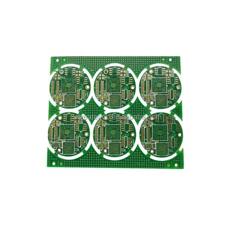
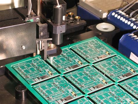
Content: Printed circuit board (PCB) is the support for circuit elements and devices in electronic products. It provides electrical connections between circuit elements and devices. With the rapid development of electronic technology, the density of PCB is getting higher and higher. The quality of PCB design has a great impact on the anti-interference ability. Therefore, when designing PCB, the general principles of PCB design must be followed and the requirements of anti-interference design must be met.
General principles of PCB design
To achieve the best performance of electronic circuits, the layout of components and wires is very important. In order to design a PCB with good quality and low cost, the following general principles should be followed:
1.Layout
First, consider the size of the PCB. When the PCB size is too large, the printed lines are long, the impedance increases, the anti-noise ability decreases, and the cost increases; if it is too small, the heat dissipation is not good, and the adjacent lines are susceptible to interference. After determining the PCB size, determine the location of special components. Finally, layout all components of the circuit according to the functional units of the circuit.
The following principles should be followed when determining the location of special components:
(1) Keep the connection between high-frequency components as short as possible, and try to reduce their distributed parameters and mutual electromagnetic interference. Components susceptible to interference should not be placed too close to each other, and input and output components should be kept as far away as possible.
(2) There may be a high potential difference between some components or wires, and the distance between them should be increased to avoid discharge leading to accidental short circuits. Components with high voltage should be placed in places that are difficult to reach during debugging.
(3) Components weighing more than 15g should be fixed with a bracket and then soldered. Those large, heavy and heat-generating components should not be installed on the printed circuit board, but should be installed on the chassis bottom plate of the whole machine, and heat dissipation should be considered. Thermistors should be kept away from heating components.
(4) The layout of adjustable components such as potentiometers, adjustable inductors, variable capacitors, and micro switches should take into account the structural requirements of the whole machine.
If it is adjusted inside the machine, it should be placed in a convenient place on the printed circuit board for adjustment; if it is adjusted outside the machine, its position should be consistent with the position of the adjustment knob on the chassis panel.
(5) The space occupied by the printed plate positioning hole and the fixing bracket should be reserved.
According to the functional units of the circuit, when laying out all the components of the circuit, the following principles should be followed:
(1) Arrange the positions of each functional circuit unit according to the flow of the circuit, so that the layout is convenient for signal flow and the signal can maintain the same direction as much as possible.
(2) Take the core component of each functional circuit as the center and lay it out around it. Components should be arranged evenly, neatly and compactly on the PCB. Minimize and shorten the leads and connections between components.
(3) For circuits working at high frequencies, the distribution parameters between components should be considered. Generally, components should be arranged in parallel as much as possible in the circuit. This is not only beautiful, but also easy to assemble and solder. It is easy to mass produce.
(4) Components located at the edge of the circuit board are generally not less than 2mm away from the edge of the circuit board. The best shape of the circuit board is a rectangle. The aspect ratio is 3:2 to 4:3. When the size of the circuit board is larger than 200x150mm, the mechanical strength of the circuit board should be considered.
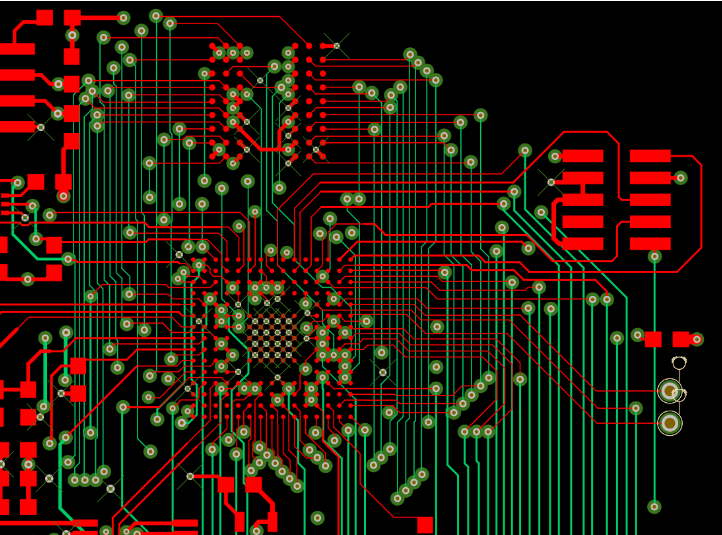
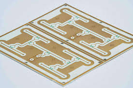
2.Wiring
The wiring principles are as follows;
(1) The wires used for input and output terminals should be avoided to be parallel to each other. It is best to add a ground wire between the wires to avoid feedback coupling.
(2) The minimum width of the printed wiring is mainly determined by the adhesion strength between the wire and the insulating substrate and the current value flowing through them.
When the copper foil thickness is 0.05mm and the width is 1~15mm.
When a current of 2A passes through, the temperature will not be higher than 3℃, so a wire width of 1.5mm can meet the requirements. For integrated circuits, especially digital circuits, a wire width of 0.02~0.3mm is usually selected. Of course, as long as it is allowed, wide wires should be used as much as possible, especially power lines and ground wires.
The minimum spacing of the wires is mainly determined by the insulation resistance and breakdown voltage between the wires in the worst case. For integrated circuits, especially digital circuits, as long as the process allows, the spacing can be as small as 5~8mm.
(3) The bends of printed conductors are generally arc-shaped, while right angles or included angles will affect the electrical performance in high-frequency circuits.
In addition, try to avoid using large-area copper foil, otherwise, when heated for a long time, the copper foil is prone to expansion and falling off. When large-area copper foil must be used, it is best to use a grid shape. This is conducive to removing the volatile gas generated by the heat of the adhesive between the copper foil and the substrate.
3.Solder pad
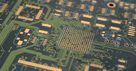
The center hole of the solder pad should be slightly larger than the diameter of the device lead. A solder pad that is too large is prone to cold soldering. The outer diameter D of the solder pad is generally not less than (d+1.2) mm, where d is the lead hole diameter. For high-density digital circuits, the minimum diameter of the solder pad can be (d+1.0) mm.
PCB and circuit anti-interference measures
The anti-interference design of printed circuit boards is closely related to the specific circuits. Here are just a few common measures for PCB anti-interference design.
(1)Power line design
According to the size of the printed circuit board current, try to increase the width of the power line and reduce the loop resistance. At the same time, make the direction of the power line and the ground line consistent with the direction of data transmission, which helps to enhance the anti-noise ability.
(2)Ground design
The principles of ground design are;
(1) Digital ground and analog ground are separated. If there are both logic circuits and linear circuits on the circuit board, they should be separated as much as possible. The ground of the low-frequency circuit should be connected to the ground at a single point in parallel as much as possible. When the actual wiring is difficult, it can be connected in series and then connected in parallel. High-frequency circuits should be grounded at multiple points in series. The ground wire should be short and loose, and a large area of grid-shaped ground foil should be used around high-frequency components as much as possible.
(2) The ground wire should be as thick as possible.
If the ground wire is made of very thin wire, the ground potential will change with the change of current, which will reduce the anti-noise performance. Therefore, the ground wire should be thickened so that it can pass three times the allowable current on the printed circuit board. If possible, the ground wire should be more than 2~3mm.
(3) The ground wire forms a closed loop.
For printed circuit boards composed only of digital circuits, the ground circuit is mostly arranged in a group loop to improve the anti-noise ability.
3.Decoupling capacitor configuration
One of the common practices in PCB design is to configure appropriate decoupling capacitors at various key locations on the printed board. The general configuration principles of decoupling capacitors are:
(1) Connect a 10~100uf electrolytic capacitor across the power input terminal. If possible, it is better to connect 100uF or more.
(2) In principle, each integrated circuit chip should be equipped with a 0.01pF ceramic capacitor. If the printed board space is insufficient, a 1~10pF capacitor can be arranged for every 4~8 chips.
(3) For devices with weak anti-noise ability and large power supply changes when turned off, such as RAM and ROM storage devices, the decoupling capacitor should be directly connected between the power line and the ground line of the chip.
(4) The capacitor lead should not be too long, especially the high-frequency bypass capacitor should not have a lead. In addition, the following two points should be noted:
(1) When there are contactors, relays, buttons and other components in the printed circuit board, they will generate large spark discharges when operating them. The RC circuit shown in the figure must be used to absorb the discharge current. Generally, R is 1~2K and C is 2.2~47UF.
(2)The input impedance of CMOS is very high and is easily inductive, so the unused end should be grounded or connected to the positive power supply when in use.