General Principles of PCB Layer Stackup Design
Introduction
Printed Circuit Board (PCB) layer stackup design is a critical aspect of modern electronics, especially as devices become more complex and require higher performance. A well-designed PCB stackup ensures signal integrity, power integrity, electromagnetic compatibility (EMC), and thermal management. This article explores the general principles of PCB layer stackup design, covering material selection, layer arrangement, impedance control, and best practices for optimal performance.
1. Understanding PCB Layer Stackup
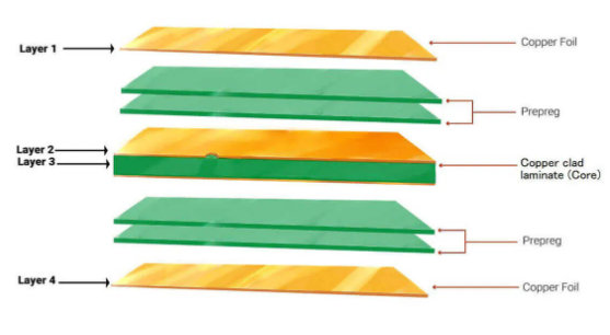
A PCB stackup refers to the arrangement of copper layers and insulating materials (dielectrics) in a multilayer PCB. The stackup defines how signals, power, and ground planes are distributed across the board. A proper stackup minimizes noise, crosstalk, and EMI while ensuring reliable power delivery and signal transmission.
Key Components of a PCB Stackup:
- Signal Layers: Carry high-speed or low-speed traces.
- Power Planes: Distribute stable voltage to components.
- Ground Planes: Provide return paths for signals and reduce EMI.
- Dielectric Layers: Insulate conductive layers (e.g., FR4, Rogers, polyimide).
2. General Principles of PCB Stackup Design
2.1. Determine the Number of Layers
The number of layers depends on:
- Circuit Complexity: High-speed designs (e.g., DDR, PCIe) require more layers.
- Signal Integrity Needs: More layers allow better controlled impedance and reduced crosstalk.
- Power Requirements: Multiple power planes may be needed for different voltage levels.
- Cost Constraints: More layers increase manufacturing costs.
Common Layer Configurations:
- 2-Layer: Simple designs (low-speed digital, analog circuits).
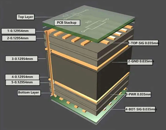
- 4-Layer: Common for moderate complexity (signal-ground-power-signal).
- 6-Layer+: High-speed designs (multiple ground/power planes for shielding).
2.2. Symmetry in Stackup
A symmetrical stackup prevents warpage and improves manufacturability. Key considerations:
- Balanced Copper Distribution: Uneven copper can cause bending during lamination.
- Matching Dielectric Thickness: Maintain uniform spacing between layers.
Example of a Symmetrical 4-Layer Stackup:
- Top Layer (Signal)
- Ground Plane
- Power Plane
- Bottom Layer (Signal)
2.3. Proper Ground and Power Plane Placement
- Adjacent Signal and Ground Planes: High-speed signals should reference a ground plane for controlled impedance.
- Avoid Power Plane Splits: Large splits can increase loop inductance and EMI.
- Use Multiple Ground Planes: Reduces noise and provides better return paths.
2.4. Controlled Impedance Design
Impedance control is crucial for high-speed signals (e.g., USB, HDMI, RF). Factors affecting impedance:
- Trace Width & Thickness
- Dielectric Constant (Dk) of Material
- Distance to Reference Plane
Common Impedance Values:
- Single-ended: 50Ω (USB, Ethernet), 75Ω (video).
- Differential Pairs: 90Ω (USB), 100Ω (Ethernet, HDMI).
2.5. Minimizing Crosstalk and EMI
- Separate High-Speed and Low-Speed Signals: Prevent interference.
- Use Ground Shielding: Place ground planes between noisy signal layers.
- Avoid Parallel Long Traces: Reduces inductive and capacitive coupling.
2.6. Thermal Management Considerations
- Copper Thickness: Thicker copper improves heat dissipation.
- Thermal Vias: Help transfer heat to inner layers or heatsinks.
- Power Plane Distribution: Avoid concentrated heat spots.
2.7. Material Selection
- FR4: Standard material for most PCBs (cost-effective, moderate performance).
- High-Frequency Materials (Rogers, Teflon): Used for RF/microwave PCBs.
- Flexible Materials (Polyimide): For flexible PCBs.
3. Best Practices for PCB Stackup Design
3.1. Start with a Reference Design
- Use manufacturer-recommended stackups for common applications (e.g., 4-layer, 6-layer).
3.2. Simulate Before Fabrication
- Use tools like SI/PI (Signal Integrity/Power Integrity) simulations to verify performance.
3.3. Follow Manufacturer Guidelines
- Consult PCB fabricators for acceptable tolerances (e.g., dielectric thickness, copper weight).
3.4. Optimize for Manufacturing Cost
- More layers = higher cost; balance performance needs with budget.
3.5. Document the Stackup Clearly
- Provide a detailed layer stackup diagram in fabrication files.
4. Common PCB Stackup Examples
4.1. 4-Layer Stackup (Common for Digital Circuits)
- Top Layer (Signal)
- Ground Plane
- Power Plane
- Bottom Layer (Signal)
Advantages:
- Good signal integrity.
- Simple and cost-effective.
4.2. 6-Layer Stackup (High-Speed Design)
- Top Layer (Signal)
- Ground Plane
- Signal Layer (High-Speed)
- Power Plane
- Ground Plane
- Bottom Layer (Signal)
Advantages:
- Better EMI shielding.
- Improved signal integrity for high-speed signals.
4.3. 8-Layer Stackup (Complex Designs)
- Top Layer (Signal)
- Ground Plane
- Signal Layer
- Power Plane
- Ground Plane
- Signal Layer
- Power/Ground Plane
- Bottom Layer (Signal)
Advantages:
- Excellent noise immunity.
- Supports multiple power domains.
5. Conclusion
Designing an optimal PCB layer stackup requires balancing signal integrity, power distribution, thermal management, and manufacturability. Key principles include:
- Using symmetrical layer arrangements.
- Proper placement of ground and power planes.
- Controlling impedance for high-speed signals.
- Minimizing crosstalk and EMI.
- Selecting appropriate materials.
By following these guidelines, engineers can ensure reliable, high-performance PCB designs for a wide range of applications.