General Requirements for PCB Panelization: Process Edges and V-Cut Guidelines
1. Introduction
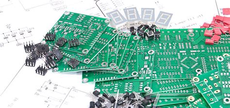
Printed Circuit Board (PCB) manufacturing often involves panelization, where multiple PCBs are fabricated on a single larger panel to optimize production efficiency. Two critical aspects of panelization are process edges (also called “breakaway tabs” or “routing tabs”) and V-cut (V-scoring). These techniques ensure that individual PCBs can be separated from the panel without damaging the circuits. This article discusses the general requirements for PCB process edges and V-cut design, including their purposes, design rules, and manufacturing considerations.
2. Purpose of Process Edges and V-Cut
2.1 Process Edges (Panelization Rails)
Process edges are extra strips of material added along the sides of a PCB panel to facilitate handling during manufacturing. They provide space for:
- Machine gripping during assembly and soldering.
- Fiducial marks for automated optical alignment.
- Tooling holes for precise drilling and layer alignment.
- Test coupons for quality control (e.g., impedance testing).
Without process edges, handling thin or small PCBs becomes difficult, leading to potential warping or misalignment.
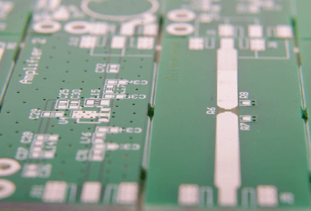
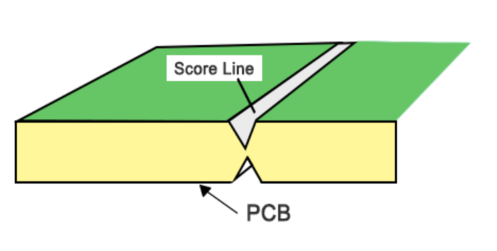
2.2 V-Cut (V-Scoring)
V-cut is a method of partially cutting the PCB panel along straight lines to allow easy separation after assembly. A V-shaped groove is created on the top and bottom of the board, leaving a thin layer of material to hold the PCBs together. Key advantages include:
- Efficient separation (boards can be snapped apart manually or with a depaneling machine).
- Space-saving compared to routing or tab-based breakaway designs.
- Smooth edges with minimal burrs.
V-cut is commonly used for rectangular PCBs, whereas complex shapes may require routing instead.
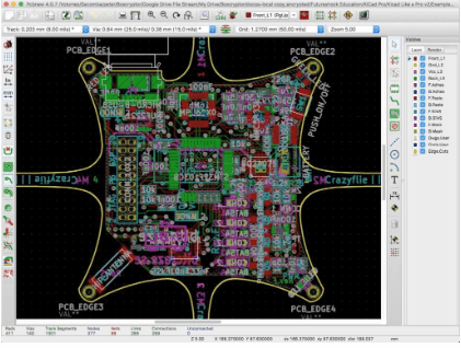
3. General Requirements for Process Edges
3.1 Width and Clearance
- Standard width: Typically 5-10 mm per side, depending on panel size and equipment requirements.
- Minimum clearance: At least 3 mm from the nearest PCB feature (traces, components, or copper pours).
- Edge grip allowance: If automated machines hold the panel, ensure no components or traces interfere with clamping areas.
3.2 Fiducial Marks and Tooling Holes
- Fiducials: At least three global fiducials (preferably in a triangular pattern) should be placed on process edges for SMT alignment.
- Tooling holes: Two or more 3.0-3.2 mm diameter holes for panel alignment during drilling and assembly.
3.3 Breakaway Tabs (if used instead of V-Cut)
- Tab width: Typically 2-5 mm with 0.5-1.0 mm mouse bites (small drilled holes) to facilitate breaking.
- Spacing between tabs: Usually 50-100 mm to ensure structural stability.
4. General Requirements for V-Cut Design
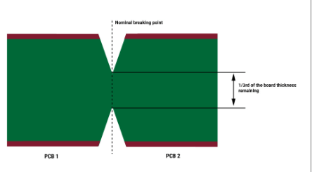
4.1 V-Cut Depth and Thickness
- Standard angle: 30° or 45° (most common).
- Remaining thickness: 1/3 of the PCB thickness (e.g., for a 1.6 mm board, leave ~0.5 mm).
- Cut tolerance: ±0.1 mm (ensure consistency to avoid incomplete cuts or excessive burring).
4.2 V-Cut Spacing and Placement
- Minimum distance from components: 2.0 mm to prevent stress damage.
- Avoid copper traces near V-cut lines: Maintain at least 0.5 mm clearance to prevent copper tearing.
- Straight-line only: V-cut cannot be used for curved or irregular separations (use routing instead).
4.3 Panel Strength Considerations
- Support bridges: If the panel is large or heavy, leave uncut sections (bridges) at intervals to prevent bending.
- Handling precautions: Avoid excessive force when depaneling to prevent cracking.
5. Manufacturing and Assembly Considerations
5.1 PCB Material and Thickness
- FR-4 standard thickness: 0.8 mm to 2.4 mm (V-cut works best in this range).
- Flexible PCBs: Not suitable for V-cut (use laser cutting or routing instead).
5.2 Depaneling Methods
- Manual breaking: Suitable for small batches but may cause rough edges.
- Automated depaneling machines: Provide cleaner cuts but require precise V-cut alignment.
- Laser cutting: Alternative for high-precision separation (no V-cut needed).
5.3 Quality Control Checks
- Visual inspection: Ensure no cracks or delamination along V-cut lines.
- Dimensional accuracy: Verify panel dimensions before depaneling.
- Burr removal: Deburring may be required after separation.
6. Common Design Mistakes to Avoid
- Insufficient process edge width → Causes handling issues during assembly.
- V-cut too deep or too shallow → Leads to difficult breaking or accidental breakage.
- Components placed too close to V-cut lines → Risk of damage during depaneling.
- No fiducials on process edges → Misalignment in SMT assembly.
- Irregular board shapes with V-cut → Only straight-line separations are possible.
7. Conclusion
Proper design of process edges and V-cut is essential for efficient PCB panelization and depaneling. Following standard guidelines ensures smooth manufacturing, reduces defects, and improves yield. Designers should collaborate with manufacturers to confirm specific requirements based on PCB thickness, assembly processes, and depaneling methods.
By adhering to these best practices, PCB manufacturers and assemblers can achieve high-quality, cost-effective production while minimizing waste and rework.