Gerber File Essentials for Streamlined PCB Prototyping
Key Takeaways
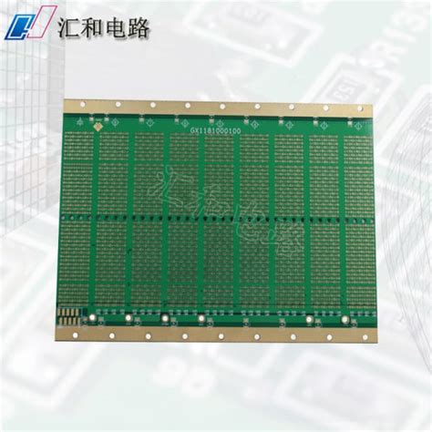
Understanding Gerber file essentials forms the foundation of successful PCB manufacturing. These files act as universal blueprints that PCB manufacturing companies rely on to translate your design intent into physical boards. When preparing Gerber files, ensure they include all necessary layers—copper, solder mask, silkscreen, and drill data—to avoid delays or misinterpretations.
Accurate Gerber data directly impacts PCB manufacturing cost by minimizing revisions and material waste. For example, misaligned drill files can lead to faulty vias, requiring costly respins. Familiarize yourself with industry standards like IPC-2581 or RS-274X to ensure compatibility with modern fabrication equipment.
While Gerber remains the default for prototyping, some PCB manufacturing business partners may request ODB++ for richer design context. Evaluate your project’s complexity: Gerber suits simpler designs, whereas ODB++ streamlines advanced layouts with embedded component data.
Always verify files using Gerber viewers before submission. Common mistakes like missing apertures or flipped layers account for over 30% of prototyping errors. By mastering these protocols, you’ll accelerate hardware iterations and build stronger collaborations with manufacturers.
Gerber Files Demystified for PCB Beginners
If you’re new to designing circuit boards, understanding Gerber files is critical for translating your ideas into functional hardware. These files act as a universal language between designers and PCB manufacturing companies, detailing every layer of your board—from copper traces to solder masks. Without accurate Gerber data, even minor errors can derail production timelines or inflate PCB manufacturing cost.
To create Gerber files correctly, start by configuring your design software to export layers in RS-274X format (the modern standard). Ensure each layer—like silkscreen, drill holes, and board outline—is labeled clearly.
Tip: Always cross-check your Gerber files using a viewer tool before sending them to manufacturers. Misaligned layers or missing apertures are common pitfalls that delay prototyping.
When collaborating with PCB manufacturing partners, clarify whether they require additional files (e.g., drill charts or pick-and-place data). Some PCB manufacturing businesses prioritize ODB++ for richer data, but Gerber remains the go-to for prototyping due to its simplicity and broad compatibility.
By mastering Gerber file creation early, you streamline communication with fabricators, reduce iterations, and keep PCB manufacturing cost predictable. This clarity not only accelerates your prototyping phase but also builds confidence in scaling projects from concept to mass production.
Why Gerber Files Matter in PCB Manufacturing
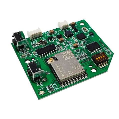
When you submit design files to pcb manufacturing companies, Gerber files act as the universal language that bridges your CAD software and fabrication equipment. These files contain precise layer-by-layer visual representations of your board, including copper traces, drill holes, and solder masks. Without accurate Gerber data, manufacturers can’t interpret your design intent, leading to costly errors or delays in pcb manufacturing.
This standardized format ensures consistency across different software tools and production systems, which is critical for maintaining quality while controlling pcb manufacturing cost. For instance, a missing solder mask layer in your Gerber files might force the fab house to request revisions, adding days to your timeline. By providing complete, error-free Gerber files, you streamline communication with pcb manufacturing business partners, reducing misinterpretation risks and accelerating prototyping cycles.
Moreover, industry-standard Gerber formats (RS-274X or X2) enable manufacturers to automate processes like panelization and optical inspection. This automation not only improves precision but also scales efficiently for high-volume orders—a key advantage when collaborating with global pcb manufacturing companies. In short, mastering Gerber file creation isn’t just about technical compliance; it’s about building a reliable foundation for turning complex designs into functional hardware.
Step-by-Step Gerber File Creation Guide
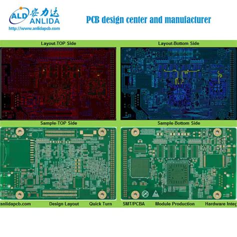
Creating Gerber files requires meticulous attention to design specifications and manufacturing requirements. Begin by exporting your PCB layout from your design software (e.g., KiCad, Altium, or Eagle), ensuring all layers—copper traces, solder masks, and silkscreens—are correctly defined. Verify your design rules match the capabilities of PCB manufacturing companies to avoid costly revisions.
Next, generate individual Gerber files for each layer, adhering to RS-274X standards. Include critical files like Top Copper, Bottom Copper, and Drill Drawing, naming them clearly (e.g., TopLayer.GTL or DrillMap.TXT). For drill data, export an Excellon format file with tool sizes and hole coordinates—this ensures compatibility with automated drilling systems.
Before finalizing, use a Gerber viewer (like ViewMate or GC-Prevue) to validate layer alignment and missing elements. Even minor errors—such as unconnected pads or overlapping traces—can increase PCB manufacturing cost or delay prototyping. Double-check that annular rings and clearances meet your manufacturer’s tolerances.
When submitting files to a PCB manufacturing business, compress all relevant files into a single ZIP folder, including a readme.txt with layer descriptions. This minimizes back-and-forth communication and accelerates production timelines. By following these steps, you’ll streamline collaboration with manufacturers while reducing risks of fabrication errors.
Gerber vs ODB: Format Selection Tips
When preparing files for PCB manufacturing, choosing between Gerber and ODB++ formats hinges on balancing compatibility and data richness. While Gerber files (RS-274X) remain the industry standard for PCB manufacturing companies due to their universal acceptance, ODB++ offers a consolidated dataset with embedded layer stackups, netlists, and material specifications. For prototyping, Gerber’s simplicity ensures fewer interpretation errors, especially when working with new manufacturers unfamiliar with ODB++’s structure. However, if your design involves complex HDI boards or tight PCB manufacturing cost constraints, ODB++’s single-source approach reduces file transfer errors and accelerates feedback cycles.
Consider your partner’s capabilities: many PCB manufacturing business operations still rely on legacy systems optimized for Gerber. Yet, adopting ODB++ early can future-proof workflows as more advanced fabrication houses embrace intelligent formats. If cost optimization is critical, verify whether your manufacturer charges extra for ODB++ processing—some offset this by reducing manual data reconstruction time. Always cross-check output files using Gerber viewers or CAM software before submission, regardless of format, to avoid costly respins.
Essential Gerber Standards for Prototyping
When preparing Gerber files for prototyping, adhering to industry-recognized standards ensures PCB manufacturing companies can accurately interpret your design intent. The RS-274X (Extended Gerber) format remains the gold standard, supporting aperture definitions and layer-specific data—critical for avoiding misinterpretations that delay production. For multi-layer boards, include IPC-2581-compliant drill tables to specify hole sizes and locations, which directly impacts PCB manufacturing cost by reducing material waste.
| Standard | Purpose | Prototyping Impact |
|---|---|---|
| RS-274X | Defines copper layers & apertures | Eliminates aperture mismatches |
| IPC-2581 | Unified data exchange format | Streamlines multi-layer validation |
| ISO 9001:2015 | Quality management compliance | Reduces rework in PCB manufacturing |
Always verify layer alignment using zero-rotation settings and confirm outline layers (GKO) match your board dimensions. Misaligned layers often lead to rejected prototypes, increasing PCB manufacturing business turnaround times. For cost-sensitive projects, ensure solder mask (GTS/GTO) and silkscreen (GTO) layers follow IPC-7351 pad-to-mask spacing rules to avoid over-etching. By embedding these standards early, you create files that align with global fabrication workflows, accelerating approvals and minimizing prototyping iterations.
Avoiding Common Gerber File Mistakes
Even minor errors in Gerber file preparation can derail PCB manufacturing timelines and inflate PCB manufacturing cost. One frequent pitfall involves layer mislabeling—failing to clearly identify copper, solder mask, or silkscreen layers. This confusion forces PCB manufacturing companies to request clarifications, adding days to turnaround times. Always verify layer naming conventions match your manufacturer’s requirements.
Another oversight is omitting critical files, such as drill charts or aperture lists. Without these, fabrication teams can’t accurately interpret hole sizes or trace widths, risking board functionality. Use automated verification tools to cross-check file completeness against industry standards like IPC-2581 or Gerber X2.
Improper scaling or unit mismatches (metric vs. imperial) also plague designs. A 0.1mm discrepancy in pad spacing might seem negligible but can cause solder bridging during assembly. Double-check your design software’s export settings to ensure units align with your PCB manufacturing business partner’s specifications.
Lastly, neglecting to include a readme file with fabrication notes—material preferences, finish types, or special tolerances—forces manufacturers to make assumptions. Proactive documentation reduces revision cycles, keeping projects on budget and schedule. By sidestepping these mistakes, you streamline collaboration with PCB manufacturing providers and avoid costly prototyping delays.
Accelerating Prototyping With Gerber Files
When preparing designs for PCB manufacturing, properly formatted Gerber files act as the universal language between your CAD software and fabrication equipment. By providing standardized layer-by-layer data, these files eliminate translation errors that often delay prototyping cycles. Leading PCB manufacturing companies rely on Gerber outputs to program drilling machines, configure solder masks, and verify copper patterns—processes that directly influence PCB manufacturing cost and turnaround times.
To maximize efficiency, ensure your Gerber set includes all critical layers (copper, silkscreen, solder mask) alongside drill files and a detailed readme. Modern CAM tools automatically flag mismatched apertures or missing layers, but cross-checking alignment and layer naming against your manufacturer’s specifications prevents costly respins. For PCB manufacturing business partners handling high-mix orders, clear Gerber documentation reduces pre-production queries by 60% or more, according to industry benchmarks.
Adopting version-controlled file management further streamlines collaboration. When submitting revisions, maintain consistent file naming and include a changelog to help manufacturers identify modifications quickly. This approach not only accelerates prototyping but builds trust with fabrication partners, ensuring your boards move from design validation to market launch without avoidable delays.
Best Practices for Gerber-Based PCB Design
When preparing Gerber files for PCB manufacturing, start by verifying your design tool’s export settings align with your manufacturer’s specifications. Most PCB manufacturing companies require RS-274X (Extended Gerber) files, which include aperture definitions and layer-specific data. Organize layers logically—labeling copper, solder mask, and silkscreen clearly—to avoid misinterpretation during fabrication.
Always include a drill file (Excellon format) with accurate tool sizes and hole coordinates. Missing or mismatched drill data is a common cause of delays, increasing PCB manufacturing cost due to rework. Use design rule checks (DRC) to flag issues like unconnected pads or insufficient clearances before exporting. For complex designs, add a readme.txt file detailing layer stackups or special requirements—this reduces back-and-forth communication with your PCB manufacturing business partner.
Prioritize consistency in naming conventions (e.g., TopLayer.gbr, BottomMask.gbr) to streamline file processing. Avoid overlapping geometries, which can confuse photoplotters, and ensure vector-based fills instead of rasterized images for sharp outlines. Finally, validate your Gerber files using free viewers like GerberLogix or manufacturer-provided tools to catch visual discrepancies early. By refining these practices, you’ll minimize errors and align with industry standards, accelerating prototyping without compromising quality.
Conclusion
When preparing files for PCB manufacturing, remember that your Gerber data acts as the universal language between design and production. Properly formatted files not only reduce errors but also enable PCB manufacturing companies to process orders faster, directly impacting your project’s timeline and PCB manufacturing cost. By adhering to industry standards like RS-274X and double-checking layer alignment, you minimize risks that could derail prototyping or escalate expenses.
Your choice to prioritize Gerber file accuracy pays dividends across the PCB manufacturing business, whether you’re iterating prototypes or scaling to mass production. Tools like automated DFM checks and clear layer naming ensure seamless communication with fabricators, while avoiding oversights like missing drill files keeps projects on track. For hardware teams, this precision translates to fewer respins, faster validation cycles, and ultimately, shorter paths to market-ready products.
Always confirm your manufacturer’s specific requirements—some may request supplemental files like pick-and-place data or IPC netlists. This proactive approach strengthens collaboration, ensuring your design intent survives the transition from screen to board. By mastering these details, you position yourself to leverage PCB manufacturing efficiencies, whether optimizing for cost-sensitive prototypes or high-reliability end products.
FAQs
Q: Why do PCB manufacturing companies require Gerber files?
A: PCB manufacturing companies rely on Gerber files to accurately interpret your design specifications. These files contain layer-by-layer details like copper traces, drill holes, and solder masks, ensuring your prototype matches your digital design exactly.
Q: How can I verify my Gerber files before sending them to a PCB manufacturing business?
A: Use Gerber viewers like ViewMate or KiCad’s built-in tools to inspect layers visually. Double-check PCB manufacturing cost factors like board dimensions and layer count, as errors here may lead to delays or additional charges.
Q: What’s the difference between RS-274X and older Gerber formats for PCB manufacturing?
A: RS-274X (Extended Gerber) supports aperture macros and embedded metadata, reducing manual input for PCB manufacturing teams. Older formats like RS-274D lack these features, increasing the risk of misinterpretation.
Q: How do Gerber files impact PCB manufacturing cost?
A: Properly optimized Gerber files minimize material waste and reduce revisions. For example, clear solder mask definitions prevent misaligned coatings, avoiding costly respins. Always confirm your PCB manufacturing company’s design rules upfront.
Q: Can ODB++ files replace Gerber in PCB manufacturing workflows?
A: While ODB++ offers unified data packaging, many PCB manufacturing businesses still prefer Gerber due to its universal compatibility. Check your manufacturer’s format requirements to avoid compatibility issues.
Q: What common Gerber mistakes delay prototyping?
A: Missing layers, incorrect aperture settings, or omitted drill files are frequent culprits. Use automated DFM checks to flag issues before submitting files to your PCB manufacturing partner.
Ready to Streamline Your PCB Manufacturing Process?
For expert guidance on Gerber file preparation and cost-effective prototyping solutions, please click here to connect with our engineering team.