H 60 pcb
Understanding the H60 PCB: A Comprehensive Guide
The H60 PCB, or printed circuit board, is a crucial component in the realm of electronics, serving as the backbone for a wide array of devices. Understanding its intricacies is essential for anyone involved in electronics design or manufacturing.
At its core, the H60 PCB is a platform that facilitates the connection of various electronic components, allowing them to communicate and function as a cohesive unit. This is achieved through a network of conductive pathways, or traces, which are etched onto a non-conductive substrate. These traces form the electrical connections between components, enabling the flow of electricity and the execution of complex tasks.
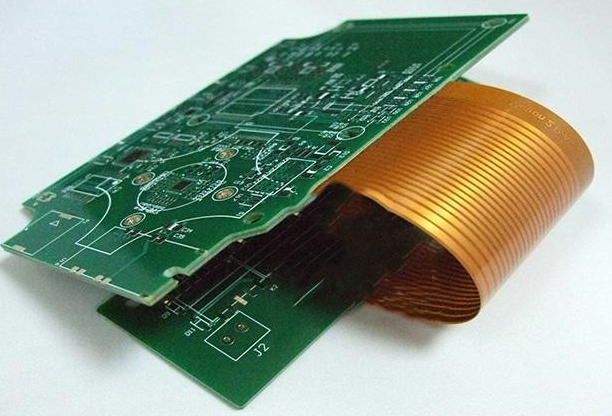
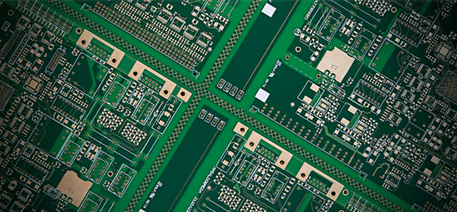
One of the defining characteristics of the H60 PCB is its multi-layered structure.
Unlike single-layer PCBs, which are limited in their capacity to accommodate complex circuits, the H60 PCB can support multiple layers of traces. This multi-layered design allows for greater density and complexity, making it ideal for advanced applications such as computer motherboards, smartphones, and other sophisticated electronic devices. The layers are separated by insulating materials, which prevent electrical interference and ensure the integrity of the signals being transmitted.
In addition to its structural complexity, the H60 PCB is also notable for its versatility.
It can be customized to meet the specific needs of different applications, with variations in size, shape, and material composition. This adaptability is particularly important in industries where space constraints and environmental conditions play a significant role in design considerations. For instance, in aerospace applications, the H60 PCB must be lightweight yet durable, capable of withstanding extreme temperatures and vibrations. Similarly, in medical devices, the PCB must be compact and reliable, ensuring consistent performance in critical situations.
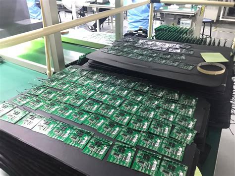
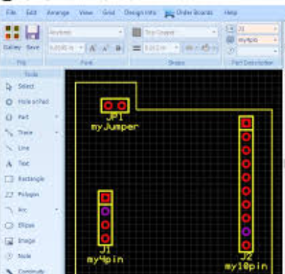
The manufacturing process of the H60 PCB is a meticulous one, involving several stages to ensure precision and quality.
It begins with the design phase, where engineers use specialized software to create a schematic of the circuit. This schematic is then translated into a layout, which serves as a blueprint for the PCB. The layout is used to produce a photomask, which is employed in the etching process to create the traces on the substrate. Following this, components are mounted onto the PCB through a process known as soldering, which involves the use of a molten metal alloy to secure the components in place.
Quality control is a vital aspect of H60 PCB production, as even minor defects can lead to significant malfunctions.
Rigorous testing is conducted at various stages of the manufacturing process to identify and rectify any issues. This includes visual inspections, electrical testing, and functional testing, all of which are designed to ensure that the PCB meets the required specifications and standards.
In conclusion, the H60 PCB is an indispensable element in modern electronics, offering a combination of complexity, versatility, and reliability. Its multi-layered design and customizable nature make it suitable for a wide range of applications, from consumer electronics to industrial machinery. Understanding the intricacies of the H60 PCB, from its structural components to its manufacturing process, is essential for anyone involved in the field of electronics, as it provides the foundation upon which innovative and efficient devices are built.

Top Features of the H60 PCB for Custom Keyboards
The H60 PCB, a popular choice among custom keyboard enthusiasts, stands out due to its impressive array of features that cater to both functionality and customization. As the heart of any keyboard, the printed circuit board (PCB) plays a crucial role in determining the overall performance and user experience. The H60 PCB, in particular, has garnered attention for its versatility and adaptability, making it a preferred option for those looking to build a personalized keyboard setup.
One of the most notable features of the H60 PCB is its support for a wide range of layouts.
This flexibility allows users to experiment with different key configurations, accommodating various typing preferences and ergonomic needs. Whether one prefers a compact 60% layout or a more traditional arrangement, the H60 PCB provides the necessary support to achieve the desired setup. This adaptability is further enhanced by the PCB’s compatibility with both ANSI and ISO standards, ensuring that users across different regions can enjoy a seamless experience.
In addition to its layout versatility, the H60 PCB is equipped with hot-swappable sockets, a feature that significantly enhances the ease of customization.
Hot-swappable sockets allow users to change switches without the need for soldering, making it convenient to test different switch types and find the perfect match for one’s typing style. This feature not only saves time but also reduces the risk of damaging the PCB during switch changes, thus extending the lifespan of the keyboard.
Moreover, the H60 PCB supports per-key RGB lighting, a feature that has become increasingly popular among keyboard enthusiasts.
This capability allows users to customize the lighting effects for each individual key, creating a visually stunning and personalized aesthetic. The integration of RGB lighting is complemented by software compatibility, enabling users to program and control the lighting effects with ease. This level of customization extends beyond mere aesthetics, as it can also enhance functionality by providing visual cues for specific key functions or shortcuts.
Another significant advantage of the H60 PCB is its robust build quality.
Constructed with high-quality materials, the PCB is designed to withstand the rigors of daily use while maintaining optimal performance. This durability is crucial for users who rely on their keyboards for both work and leisure, ensuring that the H60 PCB remains a reliable component in their setup. Furthermore, the PCB’s design incorporates features that enhance its stability and reduce the likelihood of electrical interference, contributing to a smoother and more consistent typing experience.
In conclusion, the H60 PCB offers a comprehensive suite of features that make it an ideal choice for custom keyboard builders. Its support for various layouts, hot-swappable sockets, per-key RGB lighting, and robust build quality collectively contribute to its reputation as a versatile and reliable component. As the demand for personalized and high-performance keyboards continues to grow, the H60 PCB stands out as a testament to the innovation and adaptability that define the custom keyboard community. Whether one is a seasoned enthusiast or a newcomer to the world of custom keyboards, the H60 PCB provides the tools necessary to create a truly unique and satisfying typing experience.
How to Build a Custom Keyboard with the H60 PCB
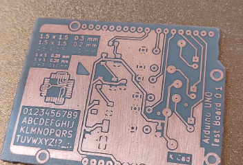
Building a custom keyboard can be a rewarding endeavor for enthusiasts seeking a personalized typing experience. At the heart of this process is the printed circuit board (PCB), which serves as the foundation for the keyboard’s functionality. The H60 PCB is a popular choice among hobbyists due to its versatility and compatibility with various layouts. Understanding how to build a custom keyboard with the H60 PCB involves several key steps, each requiring careful attention to detail.
To begin with, selecting the right components is crucial.
The H60 PCB supports a 60% keyboard layout, which is compact and ideal for those who prefer a minimalist design. This PCB is compatible with a wide range of switches, allowing users to choose from tactile, linear, or clicky options based on their typing preferences. Additionally, the H60 PCB supports both ANSI and ISO layouts, providing flexibility in key placement and design. Once the switches are selected, it is important to gather other essential components, such as stabilizers, keycaps, and a suitable case that complements the PCB.
Transitioning to the assembly process, the first step involves preparing the PCB by installing the stabilizers.
Stabilizers are necessary for larger keys, such as the spacebar and shift keys, to ensure they function smoothly without wobbling. It is advisable to test the stabilizers before proceeding, as this can prevent potential issues later in the build. Following this, the switches can be mounted onto the PCB. The H60 PCB typically features a hot-swappable design, allowing switches to be easily inserted without soldering. This feature is particularly beneficial for those who wish to experiment with different switch types.
Once the switches are securely in place, the next phase involves connecting the PCB to the case.
It is essential to ensure that the PCB is properly aligned with the case to avoid any misalignment that could affect the keyboard’s performance. After securing the PCB within the case, the keycaps can be installed. Keycaps come in various profiles and materials, offering an opportunity to further customize the keyboard’s aesthetic and feel. It is important to carefully place each keycap onto its corresponding switch to ensure proper functionality.
As the assembly nears completion, attention must be given to the firmware.
The H60 PCB is compatible with QMK firmware, a popular choice among keyboard enthusiasts for its extensive customization options. By flashing the appropriate firmware onto the PCB, users can program key functions, create macros, and customize lighting effects if the PCB supports RGB lighting. This step is crucial for tailoring the keyboard to meet individual needs and preferences.
Finally, testing the keyboard is imperative to ensure all components are functioning as expected.
This involves checking each key for responsiveness and verifying that all programmed functions operate correctly. Any issues identified during testing can often be resolved by revisiting earlier steps, such as reseating switches or re-flashing the firmware.
In conclusion, building a custom keyboard with the H60 PCB is a meticulous process that offers a unique opportunity to create a personalized typing tool. By carefully selecting components, methodically assembling the keyboard, and customizing the firmware, enthusiasts can craft a keyboard that not only meets their functional needs but also reflects their personal style. The H60 PCB, with its flexibility and user-friendly features, serves as an excellent foundation for this creative endeavor.
Troubleshooting Common Issues with the H60 PCB
The H60 PCB, a popular choice among electronics enthusiasts and professionals alike, is known for its versatility and reliability. However, like any complex electronic component, it can occasionally present users with challenges that require troubleshooting. Understanding these common issues and their solutions can significantly enhance the user experience and ensure the longevity of the device.
One of the most frequently encountered problems with the H60 PCB is connectivity issues.
These can manifest as intermittent connections or complete failure to establish a connection. Often, the root cause of such issues lies in poor soldering or damaged traces on the board. To address this, it is advisable to inspect the solder joints carefully. A magnifying glass or microscope can be particularly useful in identifying cold solder joints or bridges. Re-soldering these connections with precision can often resolve the problem. Additionally, checking for any visible damage to the traces and repairing them with conductive ink or wire can restore functionality.
Another common issue is power-related problems, which can prevent the H60 PCB from functioning correctly.
These issues may arise from a faulty power supply or incorrect voltage levels being delivered to the board. To troubleshoot power issues, it is essential to verify that the power supply is functioning correctly and delivering the appropriate voltage. Using a multimeter to measure the voltage at various points on the PCB can help identify discrepancies. If the power supply is found to be faulty, replacing it with a reliable unit is recommended. Furthermore, ensuring that all components on the board are rated for the supplied voltage can prevent future power-related issues.
Signal integrity problems can also plague the H60 PCB, leading to erratic behavior or data corruption.
These issues are often caused by electromagnetic interference (EMI) or improper grounding. To mitigate signal integrity problems, it is crucial to ensure that the PCB is properly grounded. This can be achieved by checking the ground connections and ensuring they are secure and free from corrosion. Additionally, using shielded cables and maintaining a clean layout with minimal crosstalk can help reduce EMI. In cases where signal integrity issues persist, employing ferrite beads or chokes can further suppress unwanted noise.
Component failure is another potential issue that users of the H60 PCB may encounter.
Over time, components such as capacitors, resistors, and integrated circuits can degrade or fail, leading to malfunction. To diagnose component failure, it is beneficial to perform a visual inspection for any signs of damage, such as burnt or swollen components. Testing individual components with appropriate tools, such as an LCR meter for capacitors and resistors, can confirm their functionality. Replacing any faulty components with high-quality replacements can restore the PCB to optimal performance.
In conclusion, while the H60 PCB is a robust and reliable component, it is not immune to issues that can affect its performance. By understanding and addressing common problems such as connectivity issues, power-related problems, signal integrity challenges, and component failures, users can ensure that their H60 PCB continues to operate effectively. Employing systematic troubleshooting techniques and maintaining a proactive approach to maintenance can significantly enhance the longevity and reliability of this versatile electronic component.