H bridge pcb layout
Optimizing H Bridge PCB Layout for Efficient Power Management
Optimizing the layout of an H-bridge on a printed circuit board (PCB) is crucial for efficient power management, particularly in applications involving motor control and power conversion. The H-bridge configuration, which allows for the control of current direction through a load, is a fundamental component in many electronic devices. Therefore, understanding the intricacies of its PCB layout can significantly enhance performance and reliability.
To begin with, the placement of components is a critical factor in optimizing an H-bridge PCB layout.
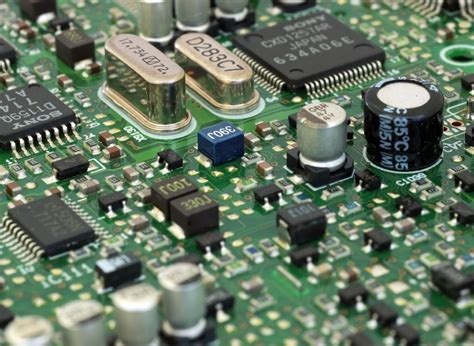
It is essential to position the power components, such as MOSFETs or IGBTs, as close to each other as possible. This minimizes the length of the current path, thereby reducing parasitic inductance and resistance. Consequently, this reduction in parasitic elements helps in minimizing power losses and improving the overall efficiency of the system. Additionally, placing decoupling capacitors near the power supply pins of the H-bridge can further stabilize the voltage levels, ensuring smooth operation.
Moreover, the routing of traces on the PCB plays a significant role in the performance of an H-bridge.
Wide and short traces are preferred for carrying high currents, as they reduce resistive losses and heat generation. It is advisable to use copper pours or planes for power and ground connections to provide a low-impedance path for current flow. This not only aids in efficient power distribution but also helps in heat dissipation, which is crucial for maintaining the thermal stability of the system.
Transitioning to the topic of thermal management, it is imperative to consider the heat generated by the H-bridge during operation.
Effective thermal management can be achieved by incorporating thermal vias and heat sinks into the PCB design. Thermal vias facilitate the transfer of heat from the top layer to the bottom layer or to an internal layer, where it can be dissipated more effectively. Heat sinks, on the other hand, provide a means to dissipate heat into the surrounding environment, thus preventing overheating and potential damage to the components.
In addition to thermal considerations, electromagnetic interference (EMI) is another aspect that must be addressed in the PCB layout.
EMI can lead to signal integrity issues and affect the performance of the H-bridge. To mitigate EMI, it is advisable to keep the loop areas of high-frequency signals as small as possible. This can be achieved by placing the return paths directly beneath the signal traces, thereby minimizing the loop area. Furthermore, incorporating ground planes and using differential signaling can also help in reducing EMI.
Finally, testing and validation are essential steps in the optimization process.
Once the PCB layout is complete, it is crucial to conduct thorough testing to ensure that the H-bridge operates as intended under various conditions. This includes testing for thermal performance, EMI compliance, and overall efficiency. By identifying and addressing any issues during the testing phase, one can ensure that the final product meets the desired specifications and performance criteria.
In conclusion, optimizing the PCB layout of an H-bridge is a multifaceted process that involves careful consideration of component placement, trace routing, thermal management, and EMI mitigation. By paying attention to these details, one can achieve efficient power management and enhance the performance and reliability of the H-bridge in various applications.
Common Mistakes to Avoid in H Bridge PCB Design
Designing an H-bridge PCB layout is a critical task for engineers working on motor control applications. The H-bridge circuit is essential for controlling the direction and speed of a motor, making it a fundamental component in robotics, automotive systems, and various industrial applications. However, designing an effective H-bridge PCB layout can be challenging, and several common mistakes can compromise the performance and reliability of the circuit. By understanding these pitfalls, engineers can create more efficient and robust designs.
One of the most frequent mistakes in H-bridge PCB design is inadequate thermal management.
H-bridges often handle significant current, which can generate substantial heat. If this heat is not properly dissipated, it can lead to component failure or reduced efficiency. To mitigate this, designers should ensure that there is sufficient copper area for heat dissipation and consider using thermal vias to transfer heat to other layers of the PCB. Additionally, incorporating heat sinks or thermal pads can further enhance heat management.
Another common error is poor component placement, which can lead to increased electromagnetic interference (EMI) and signal integrity issues.
Placing components too close together can cause crosstalk and other unwanted interactions. To avoid this, it is crucial to maintain adequate spacing between components and to follow best practices for signal routing. For instance, keeping power and ground traces as short and wide as possible can help minimize inductance and resistance, thereby reducing EMI.
Furthermore, neglecting to include adequate decoupling capacitors is a mistake that can significantly impact the performance of an H-bridge circuit.
Decoupling capacitors are essential for stabilizing the power supply and reducing voltage fluctuations. Without them, the circuit may experience noise and instability, particularly during high-current switching events. It is advisable to place decoupling capacitors as close as possible to the power pins of the H-bridge ICs to maximize their effectiveness.
In addition to these issues, improper grounding can also pose significant challenges in H-bridge PCB design.
A common mistake is failing to implement a solid ground plane, which can lead to ground loops and increased noise. A continuous ground plane helps to provide a low-impedance path for return currents, thereby improving the overall performance of the circuit. Designers should also pay attention to the placement of vias and ensure that they do not disrupt the integrity of the ground plane.
Moreover, overlooking the importance of trace width and spacing can result in excessive voltage drops and overheating.
The trace width should be calculated based on the expected current load to ensure that it can handle the required current without excessive resistance. Similarly, maintaining appropriate spacing between traces is crucial to prevent short circuits and ensure reliable operation.
Finally, failing to conduct thorough design reviews and simulations is a mistake that can lead to costly revisions and delays.
By using simulation tools, designers can identify potential issues before the PCB is manufactured, allowing for adjustments to be made early in the design process. Regular design reviews with peers can also provide valuable insights and help catch errors that may have been overlooked.
In conclusion, avoiding these common mistakes in H-bridge PCB design requires careful attention to detail and adherence to best practices. By focusing on thermal management, component placement, decoupling, grounding, trace design, and thorough testing, engineers can create efficient and reliable H-bridge circuits that meet the demands of their applications.
Advanced Techniques for Noise Reduction in H Bridge PCB Layout
In the realm of electronic circuit design, the H bridge configuration is a fundamental component used to control the direction of current flow in a load, such as a motor. However, one of the challenges faced by engineers when designing an H bridge printed circuit board (PCB) is managing and reducing noise, which can significantly impact the performance and reliability of the system. To address this issue, advanced techniques for noise reduction in H bridge PCB layout are essential.
To begin with, understanding the sources of noise in an H bridge circuit is crucial.
Noise can originate from various factors, including electromagnetic interference (EMI), ground loops, and switching transients. These noise sources can lead to erratic behavior, signal distortion, and even damage to the components. Therefore, implementing effective noise reduction strategies is imperative for ensuring optimal performance.
One of the primary techniques for noise reduction is the careful placement of components.
By strategically positioning components on the PCB, designers can minimize the loop area, which in turn reduces the inductance and susceptibility to EMI. For instance, placing decoupling capacitors as close as possible to the power pins of the H bridge IC can help filter out high-frequency noise. Additionally, arranging the power and ground traces in parallel and close proximity can further mitigate noise by reducing the loop area.
Moreover, the use of ground planes is another effective method for noise reduction.
A solid ground plane provides a low-impedance path for return currents, thereby minimizing ground loops and reducing EMI. It is advisable to dedicate an entire layer of the PCB to the ground plane, ensuring that it is continuous and unbroken. This approach not only aids in noise reduction but also enhances thermal management by dissipating heat more effectively.
Transitioning to another critical aspect, the routing of traces plays a significant role in noise management.
It is essential to keep the traces as short and direct as possible to minimize inductance and resistance. Furthermore, differential signal routing can be employed to reduce common-mode noise. By routing the positive and negative signals of a differential pair closely together, any noise picked up by the traces is likely to affect both signals equally, allowing it to be canceled out at the receiving end.
In addition to these techniques, the selection of appropriate components is vital.
Choosing components with low equivalent series resistance (ESR) and equivalent series inductance (ESL) can significantly reduce noise. For instance, using low-ESR capacitors for decoupling can enhance the filtering of high-frequency noise. Similarly, selecting MOSFETs with fast switching characteristics can minimize switching transients, thereby reducing noise.
Furthermore, incorporating shielding techniques can provide an additional layer of noise protection.
Enclosing sensitive components or sections of the PCB in a grounded metal shield can prevent external EMI from affecting the circuit. This approach is particularly beneficial in environments with high levels of electromagnetic interference.
In conclusion, advanced techniques for noise reduction in H bridge PCB layout are essential for achieving reliable and efficient circuit performance. By carefully considering component placement, utilizing ground planes, optimizing trace routing, selecting appropriate components, and incorporating shielding, engineers can effectively mitigate noise and enhance the overall functionality of the H bridge circuit. These strategies not only improve the performance of the system but also contribute to its longevity and robustness in various applications.

Step-by-Step Guide to Designing a Compact H Bridge PCB
Designing a compact H Bridge PCB is a meticulous process that requires careful planning and execution to ensure optimal performance and reliability. The H Bridge circuit is a fundamental component in controlling the direction of a DC motor, making it a crucial element in various electronic applications. To begin with, understanding the basic functionality of an H Bridge is essential. It consists of four switches, typically transistors or MOSFETs, arranged in an “H” configuration. This setup allows the current to flow in either direction through the motor, enabling forward and reverse motion.
The first step in designing a compact H Bridge PCB is selecting the appropriate components.
The choice of transistors or MOSFETs is critical, as they must be capable of handling the required current and voltage levels. Additionally, selecting components with low on-resistance can minimize power loss and heat generation, which is particularly important in compact designs where space for heat dissipation is limited. Once the components are selected, the next step is to create a schematic diagram. This diagram serves as a blueprint for the PCB layout and should clearly indicate the connections between components.
Transitioning from the schematic to the PCB layout involves several considerations.
One of the primary goals is to minimize the size of the PCB while ensuring that all components are adequately spaced to prevent electrical interference and overheating. To achieve this, it is advisable to use a double-sided PCB, which allows for more efficient use of space by placing components on both sides of the board. Furthermore, careful routing of traces is essential to minimize electromagnetic interference and ensure signal integrity. Placing power and ground traces as close as possible to each other can help reduce loop area and associated noise.
In addition to trace routing, the placement of components plays a significant role in the overall performance of the H Bridge.
It is important to position the transistors or MOSFETs symmetrically to ensure balanced current flow. Moreover, placing decoupling capacitors close to the power supply pins of the transistors can help stabilize the voltage and reduce noise. As the design progresses, thermal management becomes a critical consideration. Compact PCBs are prone to overheating, which can lead to component failure. To mitigate this risk, incorporating thermal vias and copper pours can enhance heat dissipation. Additionally, selecting components with integrated heat sinks or adding external heat sinks can further improve thermal performance.
Once the layout is complete, it is crucial to perform a thorough design rule check (DRC) to identify any potential issues such as trace width violations or clearance errors.
This step ensures that the PCB meets the necessary manufacturing standards and reduces the likelihood of errors during production. After addressing any issues identified in the DRC, the final step is to generate the Gerber files, which are used by manufacturers to produce the PCB.
In conclusion, designing a compact H Bridge PCB requires a comprehensive understanding of both the circuit’s functionality and the intricacies of PCB design. By carefully selecting components, optimizing the layout, and addressing thermal management, it is possible to create a reliable and efficient H Bridge that meets the demands of modern electronic applications. Through meticulous planning and attention to detail, engineers can successfully navigate the challenges of compact PCB design and deliver high-quality solutions.