Halogen-Free PCBs: A Comprehensive Guide to Eco-Friendly Circuit Board Technology
Introduction to Halogen-Free PCBs
In the rapidly evolving electronics industry, environmental concerns have become as crucial as technological advancements. Among the various green initiatives, halogen-free printed circuit boards (PCBs) have emerged as a significant development, addressing both environmental and health concerns associated with traditional PCB manufacturing.
Halogen-free PCBs are circuit boards manufactured without the use of halogenated materials, particularly brominated and chlorinated flame retardants that have been standard in the industry for decades. These conventional flame retardants, while effective, have raised substantial environmental and health concerns, prompting the electronics industry to seek safer alternatives.
The transition to halogen-free PCBs represents more than just compliance with environmental regulations—it signifies a fundamental shift toward sustainable electronics manufacturing. As consumers become more environmentally conscious and regulations more stringent, understanding halogen-free PCB technology becomes essential for designers, manufacturers, and end-users alike.
This comprehensive article explores the composition, benefits, manufacturing processes, applications, and future trends of halogen-free PCBs, providing valuable insights for professionals across the electronics industry.
Understanding Halogens in Traditional PCBs
To appreciate the significance of halogen-free PCBs, we must first examine the role of halogens in conventional circuit boards. Halogens—specifically bromine (Br) and chlorine (Cl)—have been integral components of PCB materials, primarily serving as flame retardants in the substrate materials.
In traditional FR-4 PCBs (the most common PCB material), brominated epoxy resins, particularly tetrabromobisphenol A (TBBPA), provide effective flame resistance. When exposed to fire, these brominated compounds release bromine radicals that interrupt the combustion process at the molecular level, effectively slowing or stopping flame propagation.
While effective for fire safety, these halogenated compounds present several concerns:
- Environmental Impact: When halogenated PCBs are improperly disposed of or incinerated, they can release toxic compounds including dioxins and furans—persistent organic pollutants that bioaccumulate in ecosystems.
- Health Hazards: Exposure to halogenated flame retardants has been linked to various health issues, including endocrine disruption, neurodevelopmental problems, and potential carcinogenic effects.
- Recycling Challenges: The presence of halogens complicates the recycling process of electronic waste, as special precautions must be taken to prevent the release of toxic substances.
- Corrosive Emissions: During PCB operation or failure, halogenated materials can release corrosive gases that may damage components and reduce product reliability.
The electronics industry’s recognition of these issues has driven the development of halogen-free alternatives that maintain performance while eliminating these negative impacts.
Defining Halogen-Free PCBs: Standards and Composition
The term “halogen-free” is strictly defined by international standards to ensure consistency across the industry. According to IPC-4101B, the primary standard for PCB base materials, a halogen-free laminate must meet the following criteria:
- Chlorine content ≤ 900 ppm (0.09% by weight)
- Bromine content ≤ 900 ppm (0.09% by weight)
- Total halogen content (Cl + Br) ≤ 1500 ppm (0.15% by weight)
These stringent limits ensure that materials classified as halogen-free contain only trace amounts of these elements, significantly reducing their environmental and health impacts.
Halogen-free PCBs achieve their flame retardancy through alternative chemistries, typically using:
- Phosphorus-based Compounds: These work by promoting char formation on the material surface when exposed to flame, creating a protective barrier that slows further combustion.
- Nitrogen-based Flame Retardants: Often used in synergy with phosphorus compounds, these materials release non-flammable gases when heated, diluting the concentration of flammable gases.
- Metal Hydroxides: Such as aluminum hydroxide or magnesium hydroxide, which release water vapor when heated, cooling the material and diluting flammable gases.
- Inorganic Fillers: These improve thermal stability and reduce flammability while maintaining mechanical properties.
The specific formulations vary by manufacturer, with each developing proprietary blends to achieve the optimal balance of flame resistance, electrical properties, and manufacturability.
Benefits of Halogen-Free PCBs
The adoption of halogen-free PCBs offers numerous advantages across environmental, technical, and regulatory domains:
Environmental Benefits
- Reduced Toxic Emissions: Eliminating halogens prevents the formation of dioxins and furans during disposal or accidental fires.
- Safer Recycling: Halogen-free boards simplify the e-waste recycling process and reduce hazards for recycling workers.
- Compliance with Environmental Directives: Meets requirements of RoHS (Restriction of Hazardous Substances), WEEE (Waste Electrical and Electronic Equipment), and other environmental regulations.
- Sustainable Manufacturing: Aligns with corporate social responsibility goals and green manufacturing initiatives.
Technical Advantages
- Improved Thermal Performance: Many halogen-free materials exhibit higher glass transition temperatures (Tg) than standard FR-4.
- Better Thermal Reliability: Reduced outgassing and lower coefficient of thermal expansion (CTE) enhance reliability in thermal cycling.
- Enhanced Signal Integrity: Some halogen-free materials offer improved dielectric properties for high-frequency applications.
- Reduced Corrosion: Elimination of halogens minimizes the risk of corrosive gas release during operation or failure.
Market and Regulatory Benefits
- Global Market Access: Compliance with international environmental regulations facilitates worldwide product distribution.
- Brand Enhancement: Demonstrates environmental commitment to eco-conscious consumers and business partners.
- Future-Proofing: Positions products ahead of anticipated stricter regulations on halogen use.
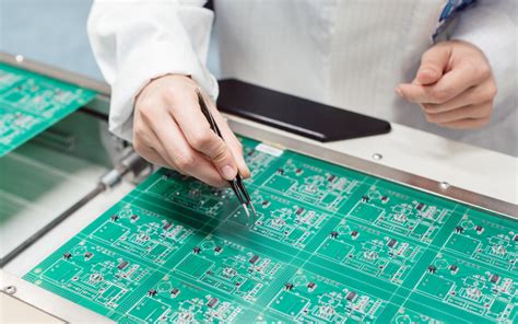
Manufacturing Halogen-Free PCBs
The production of halogen-free PCBs follows similar processes to conventional PCB manufacturing but with special considerations for material handling and processing parameters:
Material Selection
Choosing the appropriate halogen-free substrate is critical. Common halogen-free materials include:
- Halogen-free FR-4 alternatives (most common)
- Polyimide-based materials (for high-temperature applications)
- PTFE-based materials (for high-frequency applications)
- Ceramic-filled materials (for enhanced thermal performance)
Lamination Process
Halogen-free materials often require adjusted lamination parameters due to their different thermal properties:
- Typically need higher lamination temperatures
- May require modified pressure profiles
- Often benefit from longer cure times
Drilling and Machining
Halogen-free materials can be more abrasive than standard FR-4, necessitating:
- Special drill bits with enhanced wear resistance
- Adjusted drilling parameters (speed, feed rate)
- More frequent tool replacement
Surface Finishing
Common halogen-free compatible finishes include:
- Immersion silver
- Immersion tin
- Organic solderability preservatives (OSP)
- Electroless nickel/immersion gold (ENIG)
Soldering Considerations
Halogen-free PCBs may require:
- Slightly higher soldering temperatures
- Modified flux formulations
- Adjusted reflow profiles
Quality control for halogen-free PCBs includes verification of halogen content through techniques like:
- X-ray fluorescence (XRF) spectroscopy
- Ion chromatography
- Combustion ion chromatography
Applications of Halogen-Free PCBs
Halogen-free PCB technology has found adoption across numerous industries and applications:
Consumer Electronics
- Smartphones and tablets
- Laptops and desktop computers
- Televisions and home entertainment systems
Automotive Electronics
- Engine control units
- Infotainment systems
- Advanced driver assistance systems (ADAS)
- Electric vehicle power electronics
Medical Devices
- Diagnostic equipment
- Patient monitoring systems
- Implantable devices
Industrial Electronics
- Process control systems
- Power conversion equipment
- Industrial automation
Telecommunications
- Base station equipment
- Networking hardware
- 5G infrastructure
Aerospace and Defense
- Avionics systems
- Satellite electronics
- Military communications
The common thread across these applications is the combination of environmental responsibility and high reliability requirements that halogen-free PCBs can provide.
Challenges and Considerations
While halogen-free PCBs offer numerous benefits, their adoption isn’t without challenges:
Technical Challenges
- Material Availability: Fewer material options compared to conventional FR-4.
- Higher Cost: Currently 20-30% more expensive than standard FR-4.
- Process Adjustments: Requires modifications to established manufacturing processes.
- Performance Trade-offs: Some early halogen-free materials had inferior electrical or mechanical properties.
Design Considerations
- Thermal Management: Different thermal characteristics may affect heat dissipation.
- Signal Integrity: Dielectric properties vary and must be accounted for in high-speed designs.
- Mechanical Properties: May have different flexibility or strength characteristics.
Supply Chain Factors
- Limited Suppliers: Fewer sources for halogen-free materials compared to conventional options.
- Lead Times: Potentially longer procurement times for specialty materials.
- Quality Consistency: Variability between different manufacturers’ halogen-free formulations.
Despite these challenges, ongoing advancements in material science and manufacturing processes continue to mitigate these issues, making halogen-free PCBs increasingly competitive with traditional options.
Testing and Certification
Verifying and certifying halogen-free PCBs involves several standardized tests:
Halogen Content Testing
- Combustion Ion Chromatography: Precisely measures halogen content.
- X-ray Fluorescence (XRF): Quick screening method for halogens.
Performance Testing
- Flammability Testing: UL94 vertical and horizontal burn tests.
- Thermal Reliability Testing: Thermal cycling, thermal shock, and thermal aging tests.
- Electrical Testing: Dielectric constant, dissipation factor, and insulation resistance measurements.
Certification Programs
- UL Recognition: Under UL 746E for polymeric materials.
- IPC Certification: Compliance with IPC-4101B standards.
- IEC Standards: Meeting IEC 61249-2-21 requirements.
These certifications provide assurance that halogen-free PCBs meet both environmental and performance requirements.
Future Trends in Halogen-Free PCB Technology
The halogen-free PCB market continues to evolve with several notable trends:
Material Innovations
- Nanocomposite Materials: Incorporating nano-scale fillers to enhance properties.
- Bio-based Resins: Developing flame retardants from renewable resources.
- High-Performance Formulations: Improving high-frequency and high-temperature capabilities.
Manufacturing Advancements
- Improved Process Compatibility: Easier integration with existing production lines.
- Cost Reduction: Economies of scale as adoption increases.
- Multi-functional Materials: Combining halogen-free with other advanced properties.
Market Dynamics
- Growing Demand: Increasing from 15% market share in 2020 to projected 35% by 2025.
- Regulatory Expansion: More regions adopting halogen restrictions.
- Industry Collaboration: Joint development efforts among material suppliers, manufacturers, and OEMs.
Emerging Applications
- Flexible Electronics: Halogen-free flexible PCBs for wearable devices.
- High-Density Interconnect (HDI): Advanced packaging solutions.
- 5G and mmWave: Next-generation communication technologies.
Conclusion
The transition to halogen-free PCBs represents a significant step forward in sustainable electronics manufacturing. By eliminating harmful halogenated compounds while maintaining—and in some cases enhancing—performance characteristics, this technology addresses critical environmental and health concerns without compromising functionality.
While challenges remain in terms of cost and process adaptation, the ongoing advancements in material science and manufacturing techniques are rapidly closing these gaps. As environmental regulations become more stringent and consumer demand for green electronics grows, halogen-free PCBs are poised to move from a niche alternative to industry standard.
For electronics manufacturers and designers, understanding and adopting halogen-free PCB technology is no longer just an environmental consideration—it’s a strategic business decision that aligns with global sustainability goals while meeting the technical demands of modern electronic devices.
The future of PCB technology is undoubtedly green, and halogen-free solutions are at the forefront of this transformation, offering a responsible path forward for the electronics industry as it continues to innovate and grow in an increasingly eco-conscious world.