Hardware Design Practice FPC Flexible Circuit Board Design Guide
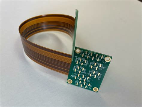
Flexible Printed Circuit (FPC Flexible Printed Circuit) is a circuit form made on a flexible surface, which can have a cover layer or not (usually used to protect the FPC circuit). Since FPC flexible circuit boards can be bent, folded or repeated in a variety of ways, they have the advantages of being light, thin and flexible compared to ordinary hard boards (PCBs), so their applications are becoming more and more extensive.
The base film material of FPC is generally polyimide (PI for short), and polyester (PET for short), with material thickness of 12.5/25/50/75/125um, and 12.5 and 25um are commonly used. If FPC needs to be soldered under high temperature conditions, its material is usually PI, and the base material of PCB is usually FR4.
The cover layer of the FPC flexible circuit board is made of a laminate of dielectric film and glue, or a coating of flexible dielectric, which has the function of preventing contamination, moisture, scratches, etc.
The main materials are the same as the base materials, namely polyimide and polyester, and the thickness of the commonly used materials is 12.5um.
When designing FPC, it is necessary to bond the layers together, and FPC adhesive is needed at this time. Common adhesives for flexible boards include acrylic, modified epoxy, phenolic butyrals, enhanced adhesive, pressure-sensitive adhesive, etc., while single-layer FPC flexible circuit boards do not need to be bonded with adhesive.
In many applications such as device welding, flexible boards need to use stiffeners to obtain external support. The main materials are PI or Polyester film, glass fiber, polymer material, steel sheet, aluminum sheet, etc.
PI or Polyester film is a commonly used material for reinforcing flexible boards, and the thickness is generally 125um. The hardness of glass fiber (FR4) reinforcement board is higher than that of PI or Polyester. It is used in places that require harder parts and is relatively difficult to process.
Compared with the processing methods of PCB pads, there are also many methods for processing FPC pads. The common ones are as follows:
① Chemical nickel gold is also called chemical immersion gold or immersion gold.
Generally, the thickness of the non-electrolytic nickel layer used on the copper metal surface of PCB is 2.5um-5.0um, and the thickness of the immersion gold (99.9% pure gold) layer is 0.05um-0.1um (previously, there was news that a PCB factory worker used the replacement method to replace the gold in the PCB pool). Advantages of this technology: flat surface, long storage time, easy to weld; suitable for fine pitch components and thinner PCBs. For FPC, it is more suitable because of its thin thickness. Disadvantages: not environmentally friendly.
② Tin-Lead Plating Advantages:
You can directly add flat lead tin to the pad, with good solderability and uniformity. For some processing techniques such as HOTBAR, this method must be used on FPC. Disadvantages: Lead is easily oxidized and has a short shelf life; electroplated wires are required; not environmentally friendly.
③ Selective gold plating (SEG) Selective gold plating refers to the use of gold plating on local areas of the PCB and another surface treatment method for other areas
. Gold plating refers to the application of a nickel layer on the copper surface of the PCB first, followed by the electroplating of a gold layer. The thickness of the nickel layer is 2.5um-5.0um, and the thickness of the gold layer is generally 0.05um-0.1um. Advantages: The gold plating layer is thicker, and has strong oxidation resistance and wear resistance. “Gold fingers” generally use this treatment method. Disadvantages: Not environmentally friendly, cyanide pollution.
④ Organic solderability protective layer (OSP) This process refers to the use of specific organic matter to cover the surface of the exposed PCB copper surface.
Advantages: It can provide a very flat PCB surface and meet environmental protection requirements. Suitable for PCBs with fine pitch components.
Disadvantages: PCBA that requires conventional wave soldering and selective wave soldering processes is not allowed to use OSP surface treatment process.
⑤ Hot air leveling (HASL) This process refers to covering the final exposed metal surface of the PCB with 63/37 lead-tin alloy.
The thickness requirement of the hot air leveling lead-tin alloy coating is 1um-25um. The hot air leveling process is more difficult to control the thickness of the coating and the pad pattern. It is not recommended to use it on PCBs with fine pitch components because fine pitch components have high requirements for pad flatness; the hot air leveling process has a greater impact on FPCs with very thin thickness, and this surface treatment method is not recommended.
In design, FPC often needs to be used in conjunction with PCB.
In the connection between the two, board-to-board connectors, connectors with gold fingers, HOTBAR, soft-hard combination boards, and manual welding are usually used for connection. For different application environments, designers can use corresponding connection methods.
In actual applications, determine whether ESD shielding is required according to application needs. When the FPC flexibility requirements are not high, solid copper and thick dielectric can be used to achieve it. When the flexibility requirement is high, copper mesh and conductive silver paste can be used.
Due to the softness of FPC flexible circuit boards, they are easy to break when subjected to stress, so some special means are needed to protect FPC.

Common methods are:
- The minimum radius of the inner angle on the flexible contour is 1.6mm. The larger the radius, the higher the reliability and the stronger the tear resistance. A trace close to the edge of the board can be added at the corner of the contour to prevent the FPC from being torn.
- The cracks or slots on the FPC must end at a circular hole with a diameter of not less than 1.5mm. This requirement also applies when the adjacent two parts of the FPC need to move separately.
- In order to achieve better flexibility, the bending area needs to be selected in an area with uniform width, and try to avoid changes in FPC width and uneven trace density in the bending area.
- Stiffener, also known as reinforcing plate, is mainly used to obtain external support. The materials used are PI, Polyester, glass fiber, polymer materials, aluminum sheets, steel sheets, etc. Reasonable design of the position, area, and material of the reinforcement plate plays a great role in preventing FPC tearing.
- When designing a multi-layer FPC, air gap layering design is required for areas that need to be bent frequently during product use. Try to use thin PI materials to increase the softness of the FPC to prevent the FPC from breaking during repeated bending.
- If space permits, a double-sided adhesive fixing area should be designed at the connection between the gold finger and the connector to prevent the gold finger and the connector from falling off during bending.
- The FPC positioning silk screen line should be designed at the connection between the FPC and the connector to prevent the FPC from being deflected or not inserted in place during assembly. It is conducive to production inspection.
Due to the particularity of FPC, the following points should be noted when routing:
Routing rules: Prioritize smooth signal routing, with short, straight, and less vias as the principle, try to avoid long, thin and winding routing, mainly horizontal, vertical and 45-degree lines, avoid arbitrary angle lines, and use curved lines for the bent parts. The above situations are described in detail as follows:
- Line width: Considering the inconsistent line width requirements for data lines and power lines, the reserved routing space is based on an average of 0.15mm
- Line spacing: According to the current production capacity of most manufacturers, the design line spacing (Pitch) is 0.10mm
- Line margin: The distance between the outermost line and the FPC outline The distance is designed to be 0.30mm, and the larger the better when space allows
- Inner fillet: The minimum value of the inner fillet on the FPC outline is designed to be a radius of R = 1.5mm
- The wire is perpendicular to the bending direction
- The wire should pass through the bending area evenly
- The wire should cover the bending area as much as possible
- There should be no additional electroplated metal in the bending area (the wire in the bending area is not electroplated)
- Keep the line width consistent
- The routing of the double-sided board cannot overlap to form an “I” shape
- The number of layers in the bending area should be minimized
- There should be no vias and metalized holes in the bending area
- The bending center axis should be set at the center of the wire. The material coefficient and thickness on both sides of the wire should be as consistent as possible. This is very important in the application of dynamic bending.
- The horizontal plane torsion follows the following principles-reducing the bending section to increase flexibility, or partially increasing the copper foil area to increase toughness.
- For vertical bending, increase the bending radius and reduce the number of layers in the center of the bending area.
- For products with EMI requirements, if high-frequency radiation signal lines such as USB and MIPI are on the FPC, a conductive silver foil layer should be added to the FPC according to the EMI measurement situation and the conductive silver foil should be grounded to prevent EMI.
As the application environment of FPC expands, the above content will continue to be enriched or inapplicable, but as long as you design carefully, think more and summarize more in your work, I believe that designing FPC is not a difficult task and you can easily get started.