Hdi pcb 2+2+2
Understanding HDI PCB: Key Features and Benefits
High-Density Interconnect (HDI) printed circuit boards (PCBs) have become a cornerstone in the advancement of modern electronics, offering a range of features and benefits that cater to the increasing demands for miniaturization and enhanced performance. Among the various configurations of HDI PCBs, the 2+2+2 structure stands out for its unique capabilities and applications. Understanding the key features and benefits of HDI PCBs, particularly the 2+2+2 configuration, is essential for appreciating their role in contemporary electronic design.
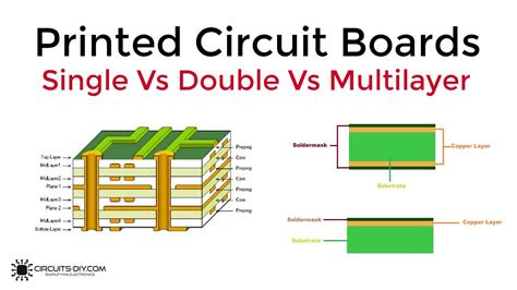
HDI PCBs are characterized by their higher wiring density per unit area compared to traditional PCBs.
This is achieved through the use of finer lines and spaces, smaller vias, and capture pads, as well as higher connection pad density. The 2+2+2 configuration refers to a specific layer structure within the PCB, consisting of two sequentially laminated layers on each side of a core. This structure allows for more complex routing and greater component density, which is particularly beneficial in applications where space is at a premium.
One of the primary features of HDI PCBs is the use of microvias, which are significantly smaller than traditional vias.
In the 2+2+2 configuration, microvias are used to connect the different layers, enabling more efficient use of space and allowing for more intricate designs. This is particularly advantageous in the development of compact devices such as smartphones, tablets, and wearable technology, where every millimeter of space is crucial. Moreover, the use of microvias reduces the parasitic capacitance and inductance, leading to improved electrical performance.
Another notable feature of HDI PCBs is their ability to support higher signal transmission speeds.
The 2+2+2 configuration, with its multiple layers and efficient interconnections, facilitates the handling of high-frequency signals with minimal loss. This is essential in applications such as telecommunications and data processing, where rapid and reliable signal transmission is critical. Additionally, the enhanced thermal management capabilities of HDI PCBs help in maintaining the integrity of high-speed signals by dissipating heat more effectively.
The benefits of HDI PCBs extend beyond their physical and electrical characteristics.
The 2+2+2 configuration also contributes to cost efficiency in the manufacturing process. By enabling more components to be placed on a single board, HDI PCBs reduce the need for additional boards and interconnections, which can lower material and assembly costs. Furthermore, the compact design of HDI PCBs can lead to reductions in the overall size and weight of the final product, which is a significant advantage in industries such as aerospace and automotive, where weight savings can translate into improved performance and fuel efficiency.
In conclusion, the 2+2+2 configuration of HDI PCBs exemplifies the advanced capabilities and benefits that these boards offer. From their ability to accommodate complex designs and high-speed signals to their cost efficiency and space-saving advantages, HDI PCBs are integral to the development of modern electronic devices. As technology continues to evolve, the demand for HDI PCBs, particularly those with sophisticated configurations like 2+2+2, is expected to grow, underscoring their importance in the future of electronic design and manufacturing.

Design Considerations for HDI PCB: Best Practices
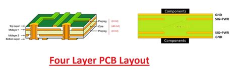
When designing High-Density Interconnect (HDI) Printed Circuit Boards (PCBs), particularly those with a 2+2+2 layer configuration, several critical considerations must be taken into account to ensure optimal performance and reliability. The 2+2+2 structure, which refers to two layers of microvias on each side of a core, offers enhanced routing capabilities and improved electrical performance. However, this complexity necessitates a meticulous approach to design.
To begin with, understanding the material selection is paramount.
The choice of substrate material can significantly impact the board’s thermal and electrical properties. Materials with high glass transition temperatures (Tg) and low coefficients of thermal expansion (CTE) are preferred, as they provide stability under thermal stress. Additionally, the dielectric constant of the material should be considered to ensure signal integrity, especially in high-frequency applications.
Transitioning to the aspect of via design, microvias play a crucial role in HDI PCBs.
In a 2+2+2 configuration, microvias are used to connect the outer layers to the inner layers, facilitating high-density routing. It is essential to adhere to the aspect ratio guidelines for microvias to maintain structural integrity and reliability. Typically, an aspect ratio of 1:1 is recommended to prevent issues such as via cracking or plating voids. Furthermore, the use of stacked or staggered microvias should be carefully evaluated based on the specific design requirements and manufacturing capabilities.
Signal integrity is another critical consideration in HDI PCB design.
As the density of the board increases, so does the potential for signal interference and crosstalk. To mitigate these issues, designers should employ techniques such as controlled impedance routing and differential pair routing. Additionally, maintaining adequate spacing between traces and incorporating ground planes can help reduce electromagnetic interference (EMI) and ensure signal clarity.
Thermal management is also a vital aspect of HDI PCB design.
The compact nature of a 2+2+2 configuration can lead to increased heat generation, which, if not properly managed, can affect the performance and longevity of the board. Implementing thermal vias, heat sinks, and thermal pads can aid in dissipating heat effectively. Moreover, selecting components with lower power consumption and optimizing the layout for efficient airflow can further enhance thermal performance.
In terms of manufacturability, collaboration with PCB manufacturers during the design phase is crucial.
Engaging with manufacturers early on can provide insights into the limitations and capabilities of the fabrication process, allowing for adjustments that can reduce costs and improve yield. Design for manufacturability (DFM) principles should be applied to ensure that the design can be produced reliably and efficiently.
Finally, testing and validation are indispensable steps in the design process.
Rigorous testing, including electrical testing and thermal cycling, can identify potential issues before mass production. Employing simulation tools during the design phase can also predict performance and highlight areas for improvement.
In conclusion, designing an HDI PCB with a 2+2+2 configuration requires a comprehensive approach that considers material selection, via design, signal integrity, thermal management, manufacturability, and testing. By adhering to best practices and leveraging advanced design tools, engineers can create robust and reliable HDI PCBs that meet the demands of modern electronic applications.
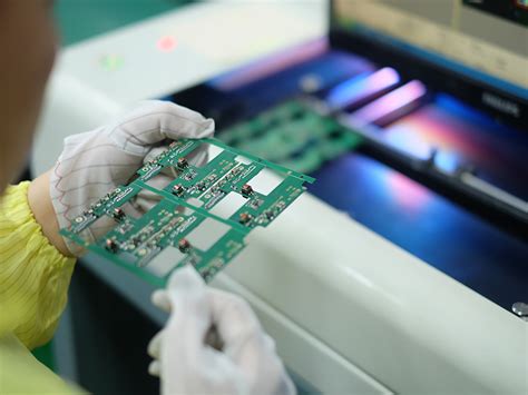
Manufacturing Process of HDI PCB: A Step-by-Step Guide
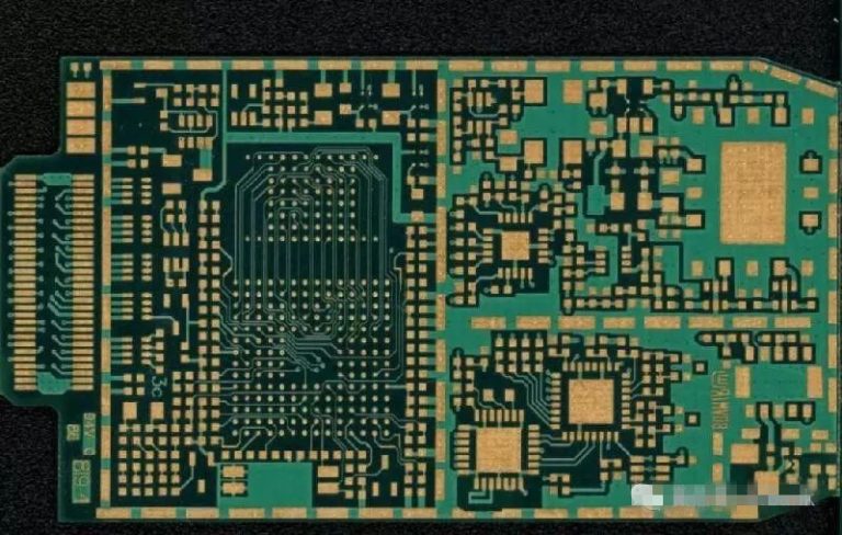
The manufacturing process of High-Density Interconnect (HDI) Printed Circuit Boards (PCBs), particularly the 2+2+2 configuration, is a sophisticated procedure that requires precision and advanced technology. This configuration, characterized by two layers of microvias on each side of the core, is designed to accommodate the increasing demand for miniaturization and enhanced performance in electronic devices. To understand the intricacies of this process, it is essential to explore each step involved, from the initial design to the final inspection.
Initially, the process begins with the design phase, where engineers utilize advanced software to create a detailed blueprint of the PCB.
This design includes the layout of the microvias, traces, and pads, ensuring that the board will meet the required electrical and mechanical specifications. Once the design is finalized, it is transferred to a photolithographic film, which serves as a template for the subsequent steps.
Following the design phase, the core material, typically a fiberglass-reinforced epoxy laminate, is prepared.
This core acts as the central layer of the 2+2+2 HDI PCB. The core is then coated with a layer of photoresist, a light-sensitive material that hardens when exposed to ultraviolet light. The photolithographic film is placed over the core, and the assembly is exposed to UV light, transferring the design onto the photoresist. The unexposed areas of the photoresist are then removed, revealing the pattern of the circuit.
Subsequently, the exposed areas of the core are etched away using a chemical solution, leaving behind the desired circuit pattern.
This etching process is critical, as it defines the electrical pathways on the PCB. Once the etching is complete, the remaining photoresist is stripped away, and the core is thoroughly cleaned to remove any residues.
The next step involves the creation of microvias, which are tiny holes that connect the different layers of the PCB.
In the 2+2+2 configuration, these microvias are drilled using a laser, which offers the precision necessary for such small features. After drilling, the microvias are plated with copper to establish electrical connections between the layers.
With the core and microvias prepared, the outer layers are laminated onto the core.
This lamination process involves pressing the layers together under heat and pressure, ensuring a strong bond. The outer layers are then subjected to the same photolithographic and etching processes as the core, creating the circuit patterns on both sides of the PCB.
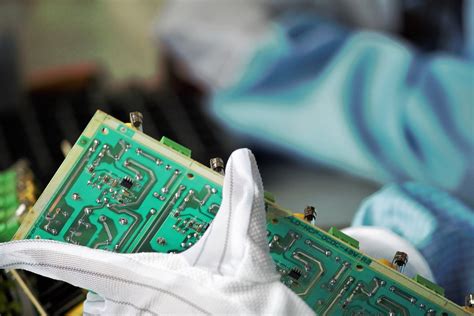
Once all layers are in place, the PCB undergoes a series of inspections and tests to ensure its functionality and reliability.
These tests include electrical testing to verify the integrity of the connections and visual inspections to detect any physical defects. Any issues identified during these inspections are addressed before the PCB is approved for use.
In conclusion, the manufacturing process of a 2+2+2 HDI PCB is a complex and meticulous procedure that combines advanced technology with precise engineering. Each step, from design to inspection, plays a crucial role in producing a high-quality PCB capable of meeting the demands of modern electronic devices. As technology continues to evolve, the methods and materials used in HDI PCB manufacturing will undoubtedly advance, further enhancing the capabilities of these essential components.
Applications of HDI PCB in Modern Electronics
High-Density Interconnect (HDI) printed circuit boards (PCBs) have become a cornerstone in the advancement of modern electronics, offering a multitude of applications that leverage their compact design and enhanced performance capabilities. The 2+2+2 configuration, a specific type of HDI PCB, is particularly noteworthy for its ability to accommodate complex circuitry within a limited space, thereby meeting the ever-growing demand for miniaturization in electronic devices. This configuration involves a multi-layered structure with two layers of circuitry on each side of the core, interconnected through microvias, which are smaller and more efficient than traditional vias. As a result, HDI PCBs are increasingly being utilized in a variety of cutting-edge applications.
One of the primary applications of HDI PCBs is in the realm of consumer electronics, where the demand for smaller, more powerful devices is relentless.
Smartphones, tablets, and wearable technology are prime examples of products that benefit from the compact and efficient design of HDI PCBs. The 2+2+2 configuration allows for more components to be packed into a smaller area, enabling manufacturers to produce devices that are not only slimmer but also more powerful. This is particularly important in the smartphone industry, where the competition to offer the most features in the smallest package is fierce. The enhanced electrical performance of HDI PCBs also contributes to faster processing speeds and improved battery life, which are critical factors for consumer satisfaction.
In addition to consumer electronics, HDI PCBs are making significant inroads into the automotive industry.
Modern vehicles are increasingly reliant on electronic systems for everything from engine control to infotainment systems. The compact nature of HDI PCBs allows for the integration of more sophisticated electronic systems without increasing the weight or size of the vehicle. This is particularly beneficial for electric vehicles, where space and weight savings can directly translate into improved range and efficiency. Furthermore, the reliability and durability of HDI PCBs make them well-suited for the harsh conditions often encountered in automotive environments.
The medical field is another area where HDI PCBs are proving invaluable.
Medical devices, such as pacemakers, hearing aids, and diagnostic equipment, require high levels of precision and reliability. The 2+2+2 HDI PCB configuration supports the miniaturization of these devices, making them less invasive and more comfortable for patients. Additionally, the ability to incorporate more functionality into a smaller footprint allows for the development of more advanced diagnostic tools, which can lead to earlier detection and more effective treatment of medical conditions.
Moreover, the aerospace and defense sectors are also capitalizing on the advantages offered by HDI PCBs.
In these industries, the need for lightweight, reliable, and high-performance electronic systems is paramount. HDI PCBs provide the necessary attributes to meet these demands, enabling the development of advanced avionics, communication systems, and other critical technologies. The 2+2+2 configuration, with its ability to support complex circuitry in a compact form, is particularly beneficial in applications where space and weight are at a premium.
In conclusion, the applications of HDI PCBs, particularly the 2+2+2 configuration, are vast and varied, spanning multiple industries and driving innovation in modern electronics. As technology continues to evolve, the role of HDI PCBs in enabling smaller, more powerful, and more efficient electronic devices is likely to expand, further cementing their importance in the future of electronic design and manufacturing.