Hdi pcb capability
Understanding HDI PCB Capability: Key Features and Benefits
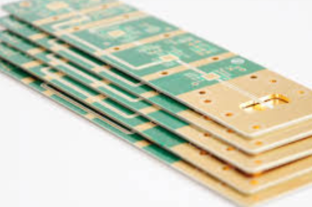
High-Density Interconnect (HDI) Printed Circuit Boards (PCBs) represent a significant advancement in the field of electronics manufacturing, offering a range of capabilities that cater to the increasing demands for miniaturization and enhanced performance. Understanding the key features and benefits of HDI PCB capability is essential for professionals in the electronics industry, as these advanced PCBs are becoming integral to modern electronic devices.
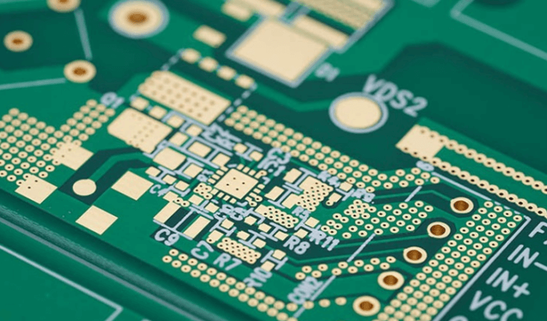
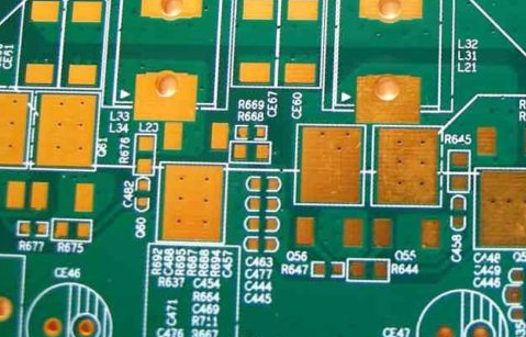
One of the primary features of HDI PCBs is their ability to support higher wiring density compared to traditional PCBs.
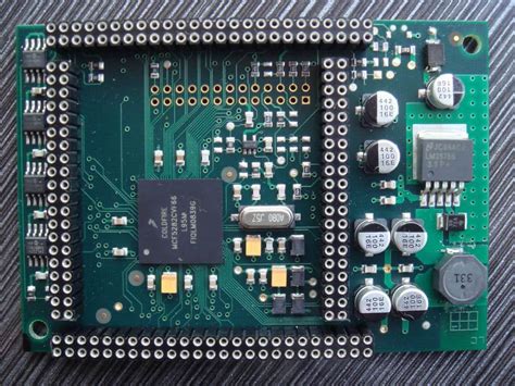
This is achieved through the use of finer lines and spaces, smaller vias, and capture pads, as well as higher connection pad density. The incorporation of microvias, which are significantly smaller than conventional vias, allows for more efficient use of the board space. These microvias can be stacked or staggered, providing designers with greater flexibility in routing complex circuits. Consequently, HDI PCBs can accommodate more components in a smaller area, making them ideal for compact devices such as smartphones, tablets, and wearable technology.
In addition to their compact size, HDI PCBs offer improved electrical performance.
The shorter signal paths enabled by the high-density interconnects reduce signal loss and electromagnetic interference (EMI), leading to faster signal transmission and better overall performance. This is particularly beneficial in high-speed applications where signal integrity is critical. Furthermore, the use of advanced materials and manufacturing processes in HDI PCBs enhances their thermal management capabilities, ensuring reliable operation even in demanding environments.
Another significant benefit of HDI PCBs is their ability to support advanced component packaging technologies, such as chip-scale packages (CSPs) and ball grid arrays (BGAs).
These packaging methods allow for a higher number of input/output (I/O) connections in a smaller footprint, further contributing to the miniaturization of electronic devices. The compatibility of HDI PCBs with these advanced packaging technologies enables the development of more powerful and feature-rich products without compromising on size or weight.
Moreover, the versatility of HDI PCBs extends to their application in various industries.
In the automotive sector, for instance, HDI PCBs are used in advanced driver-assistance systems (ADAS), infotainment systems, and other electronic control units (ECUs) that require high reliability and performance. In the medical field, HDI PCBs are found in diagnostic equipment, implantable devices, and portable medical devices, where their small size and high performance are crucial. The aerospace and defense industries also benefit from HDI PCBs, as they provide the necessary performance and reliability for mission-critical applications.
Despite the numerous advantages, it is important to acknowledge the challenges associated with HDI PCB manufacturing.
The complexity of the design and fabrication processes requires specialized equipment and expertise, which can result in higher production costs. However, the long-term benefits of improved performance, reduced size, and enhanced functionality often outweigh the initial investment, making HDI PCBs a worthwhile consideration for many applications.
In conclusion, HDI PCB capability offers a range of key features and benefits that address the growing demands for miniaturization and high performance in modern electronic devices. The ability to support higher wiring density, improved electrical performance, advanced component packaging, and versatility across various industries underscores the importance of HDI PCBs in the future of electronics manufacturing. As technology continues to evolve, the role of HDI PCBs in enabling innovative and efficient solutions will undoubtedly become even more significant.
Advanced Manufacturing Techniques for HDI PCB Capability
High-Density Interconnect (HDI) Printed Circuit Boards (PCBs) represent a significant advancement in the field of electronics manufacturing, offering enhanced performance and miniaturization capabilities. The development of HDI PCBs has been driven by the increasing demand for more compact, efficient, and powerful electronic devices. As a result, advanced manufacturing techniques have become essential to meet the stringent requirements of HDI PCB production.
One of the primary techniques employed in the manufacturing of HDI PCBs is laser drilling.
This method allows for the creation of microvias, which are small holes that connect different layers of the PCB. Laser drilling offers high precision and accuracy, enabling the production of microvias with diameters as small as 50 micrometers. This capability is crucial for HDI PCBs, as it allows for the dense interconnection of components, thereby reducing the overall size of the board while maintaining high performance.
In addition to laser drilling, the use of advanced materials is another critical aspect of HDI PCB manufacturing.
High-performance laminates and substrates, such as polyimide and liquid crystal polymer (LCP), are often used to enhance the thermal and electrical properties of the PCB. These materials provide excellent dimensional stability, low dielectric constant, and high thermal conductivity, which are essential for the reliable operation of HDI PCBs in demanding applications.
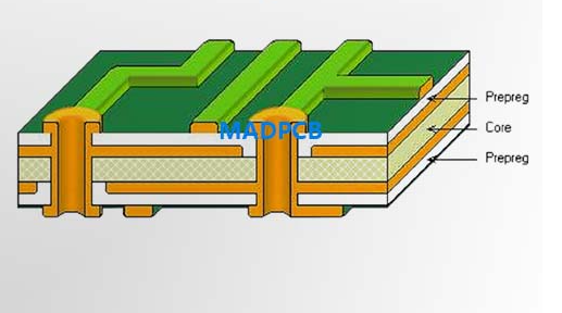
Furthermore, the implementation of sequential lamination processes is a key technique in HDI PCB manufacturing.
This process involves the repeated layering and bonding of materials to create a multi-layered PCB structure. Sequential lamination allows for the integration of multiple layers of circuitry within a compact footprint, thereby increasing the density and complexity of the PCB. This technique is particularly beneficial for applications that require high-speed signal transmission and high-frequency performance.
Another important manufacturing technique for HDI PCBs is the use of advanced plating technologies.
Electroless copper plating, for instance, is commonly used to deposit a thin layer of copper onto the surface of the PCB and within the microvias. This process ensures excellent adhesion and conductivity, which are critical for the reliable performance of HDI PCBs. Additionally, the use of advanced surface finishes, such as immersion gold and organic solderability preservatives (OSP), helps to protect the PCB from oxidation and corrosion, thereby extending its lifespan.
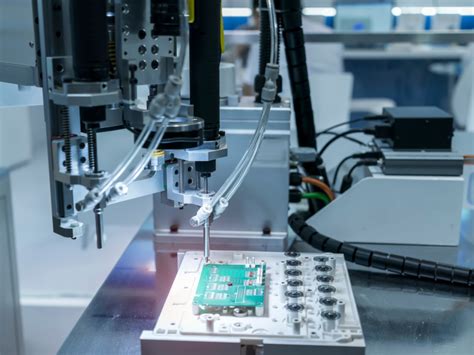
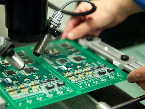
Moreover, the adoption of automated optical inspection (AOI) systems is essential for ensuring the quality and reliability of HDI PCBs.
AOI systems use high-resolution cameras and sophisticated algorithms to detect defects and inconsistencies in the PCB during the manufacturing process. This technology enables manufacturers to identify and address issues early in the production cycle, thereby reducing the risk of defects and improving overall yield.
In conclusion, the manufacturing of HDI PCBs requires the integration of advanced techniques and materials to achieve the desired performance and miniaturization. Laser drilling, advanced materials, sequential lamination, advanced plating technologies, and automated optical inspection are all critical components of the HDI PCB manufacturing process. These techniques not only enable the production of high-density, high-performance PCBs but also ensure their reliability and longevity in a wide range of applications. As the demand for more compact and powerful electronic devices continues to grow, the importance of advanced manufacturing techniques for HDI PCB capability will only become more pronounced.
Design Considerations for Maximizing HDI PCB Capability
High-Density Interconnect (HDI) Printed Circuit Boards (PCBs) have become a cornerstone in modern electronics, offering enhanced performance and miniaturization. To maximize the capabilities of HDI PCBs, several design considerations must be meticulously addressed. These considerations span from material selection to layout strategies, each playing a crucial role in the overall functionality and reliability of the final product.
Firstly, the choice of materials is paramount.
HDI PCBs often require substrates with high thermal stability and low dielectric constants to support high-speed signal transmission. Materials such as FR-4, polyimide, and advanced laminates like Rogers or Taconic are commonly used. The selection process should consider the thermal and electrical properties of these materials to ensure they meet the specific requirements of the application. Additionally, the compatibility of these materials with the manufacturing processes, such as laser drilling and sequential lamination, must be evaluated to avoid potential issues during production.
Transitioning to the layout design, the use of microvias is a defining feature of HDI PCBs.
Microvias, which are significantly smaller than traditional vias, enable higher routing density and improved signal integrity. The placement and size of these microvias must be carefully planned to optimize space utilization while maintaining structural integrity. It is essential to adhere to the design rules provided by the PCB manufacturer, as these rules dictate the minimum allowable dimensions and spacing for microvias, ensuring manufacturability and reliability.
Furthermore, the layer stack-up configuration is a critical aspect of HDI PCB design.
A well-thought-out stack-up can significantly enhance signal integrity and reduce electromagnetic interference (EMI). Typically, HDI PCBs employ a combination of core and build-up layers, with the build-up layers containing the microvias. The arrangement of these layers should facilitate efficient power distribution and signal routing while minimizing crosstalk and signal loss. Designers must also consider the impedance control requirements, which are influenced by the dielectric properties of the materials and the geometry of the traces and vias.
In addition to the physical layout, the electrical performance of HDI PCBs is heavily influenced by the design of the power and ground planes.
These planes should be strategically placed to provide a low-impedance path for return currents, thereby reducing noise and improving signal integrity. The use of multiple ground planes can further enhance performance by providing additional shielding and reducing the loop area for high-frequency signals. Careful attention to the placement of decoupling capacitors is also necessary to ensure stable power delivery to the active components.
Moreover, thermal management is a crucial consideration in HDI PCB design.
The high component density and increased power consumption can lead to significant heat generation, which must be effectively dissipated to prevent thermal damage and ensure reliable operation. Techniques such as thermal vias, heat sinks, and thermal interface materials can be employed to enhance heat dissipation. The thermal properties of the chosen substrate material also play a vital role in managing heat.
Lastly, manufacturability and testing should not be overlooked.
The complexity of HDI PCBs necessitates thorough design for manufacturability (DFM) and design for testability (DFT) practices. Collaborating closely with the PCB manufacturer during the design phase can help identify potential issues early and ensure that the design is optimized for production. Implementing test points and considering the accessibility of critical nodes can facilitate effective testing and troubleshooting.
In conclusion, maximizing the capability of HDI PCBs requires a comprehensive approach that encompasses material selection, layout design, electrical performance, thermal management, and manufacturability. By meticulously addressing these design considerations, engineers can harness the full potential of HDI technology, leading to the development of high-performance, reliable electronic products.
Comparing HDI PCB Capability with Traditional PCB Technologies
High-Density Interconnect (HDI) Printed Circuit Boards (PCBs) represent a significant advancement in the field of electronics manufacturing, offering capabilities that surpass those of traditional PCB technologies. As the demand for more compact, efficient, and high-performance electronic devices continues to grow, understanding the differences between HDI and traditional PCBs becomes increasingly important.
To begin with, HDI PCBs are characterized by their higher wiring density per unit area compared to traditional PCBs.
This is achieved through the use of finer lines and spaces, smaller vias, and capture pads, as well as higher connection pad density. These features enable HDI PCBs to support more complex and compact designs, which is particularly beneficial for modern electronic devices that require miniaturization without compromising performance. In contrast, traditional PCBs, while still widely used, often struggle to meet the demands of contemporary electronic applications due to their relatively larger feature sizes and lower density.
One of the key advantages of HDI PCBs is their ability to incorporate multiple layers of interconnections.
This is facilitated by the use of microvias, which are significantly smaller than the vias used in traditional PCBs. Microvias can be drilled using laser technology, allowing for precise and efficient creation of interlayer connections. This capability not only enhances the electrical performance of the PCB by reducing signal loss and improving signal integrity but also allows for more design flexibility. Traditional PCBs, on the other hand, typically rely on through-hole vias, which are larger and can limit the density and complexity of the design.
Moreover, HDI PCBs offer improved thermal management capabilities.
The increased density and smaller feature sizes allow for better heat dissipation, which is crucial for high-performance applications. This is particularly important in industries such as aerospace, automotive, and telecommunications, where reliable thermal management is essential for the longevity and performance of electronic components. Traditional PCBs, with their larger and less dense structures, often face challenges in effectively managing heat, which can lead to reduced performance and reliability.
In addition to these technical advantages, HDI PCBs also provide economic benefits.
Although the initial manufacturing cost of HDI PCBs can be higher due to the advanced technology and materials required, the overall cost-effectiveness is often superior in the long run. This is because HDI PCBs can reduce the need for additional components and interconnections, leading to lower assembly costs and improved reliability. Furthermore, the ability to create more compact designs can result in smaller and lighter end products, which can be a significant advantage in terms of shipping and handling costs.
It is also worth noting that the adoption of HDI PCB technology is driven by the increasing complexity of modern electronic devices. As devices become more multifunctional and feature-rich, the need for advanced PCB technologies that can support these requirements becomes more pronounced. HDI PCBs, with their superior density, performance, and reliability, are well-suited to meet these demands. Traditional PCBs, while still relevant for less complex applications, are gradually being overshadowed by the capabilities of HDI technology.
In conclusion, the comparison between HDI PCB capability and traditional PCB technologies highlights the significant advancements that HDI brings to the table. With their higher density, improved performance, better thermal management, and economic benefits, HDI PCBs are increasingly becoming the preferred choice for modern electronic applications. As technology continues to evolve, the role of HDI PCBs in shaping the future of electronics is set to become even more prominent.