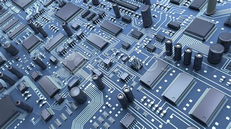
Hdi pcb construction
Understanding The Basics Of HDI PCB Construction
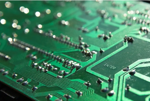
High-Density Interconnect (HDI) Printed Circuit Boards (PCBs) represent a significant advancement in the field of electronics, offering a compact and efficient solution for modern electronic devices. Understanding the basics of HDI PCB construction is essential for those involved in electronics design and manufacturing, as these boards are increasingly becoming the standard in the industry. HDI PCBs are characterized by their higher wiring density per unit area compared to traditional PCBs, which is achieved through the use of finer lines and spaces, smaller vias, and capture pads. This increased density allows for more components to be placed on both sides of the board, facilitating the creation of smaller, lighter, and more powerful electronic devices.
The construction of HDI PCBs involves several key processes that distinguish them from conventional PCBs.
One of the primary techniques used in HDI PCB construction is the use of microvias, which are significantly smaller than the vias used in traditional PCBs. Microvias are typically drilled using laser technology, allowing for precise and accurate placement. These microvias enable the interconnection of multiple layers within the PCB, which is crucial for achieving the high-density interconnectivity that HDI boards are known for. Furthermore, the use of microvias reduces the need for through-hole vias, which can take up valuable space and limit the routing options available to designers.
In addition to microvias, HDI PCBs often incorporate blind and buried vias.
Blind vias connect an outer layer to one or more inner layers but do not pass through the entire board, while buried vias connect only internal layers and are not visible from the outer surfaces. These types of vias contribute to the efficient use of space within the PCB, allowing for more complex and compact designs. The combination of microvias, blind vias, and buried vias provides designers with a versatile toolkit for creating intricate and high-performance electronic circuits.
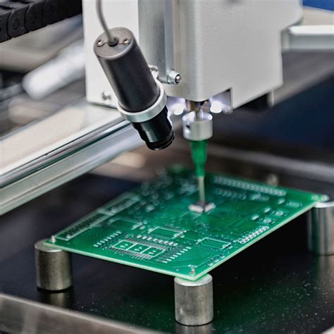
`Another important aspect of HDI PCB construction is the use of advanced materials and fabrication techniques.
The materials used in HDI PCBs must be able to withstand the higher temperatures and mechanical stresses associated with the increased component density and miniaturization. As such, high-performance laminates and substrates are often employed to ensure reliability and durability. Additionally, the fabrication process for HDI PCBs requires precise control and advanced equipment to achieve the fine lines and spaces necessary for high-density interconnectivity.
The benefits of HDI PCB construction are numerous, making them an attractive option for a wide range of applications.
The increased component density allows for the development of smaller and lighter devices, which is particularly important in industries such as consumer electronics, telecommunications, and medical devices. Moreover, the enhanced electrical performance of HDI PCBs, resulting from shorter signal paths and reduced parasitic effects, contributes to faster signal transmission and improved overall device performance.
In conclusion, understanding the basics of HDI PCB construction is crucial for those involved in the design and manufacture of modern electronic devices. The use of microvias, blind and buried vias, advanced materials, and precise fabrication techniques all contribute to the high-density interconnectivity that defines HDI PCBs. As technology continues to evolve, the demand for smaller, more powerful, and more efficient electronic devices will only increase, further solidifying the importance of HDI PCB construction in the electronics industry.
Key Materials Used In HDI PCB Manufacturing
High-Density Interconnect (HDI) printed circuit boards (PCBs) represent a significant advancement in the field of electronics manufacturing, offering enhanced performance and miniaturization capabilities. The construction of HDI PCBs involves the use of specialized materials that contribute to their superior functionality and reliability. Understanding these key materials is essential for appreciating the intricacies of HDI PCB manufacturing.
.To begin with, the substrate material forms the foundation of any PCB, and in the case of HDI PCBs, the choice of substrate is crucial.
Typically, high-performance laminates such as FR-4, a glass-reinforced epoxy laminate, are used due to their excellent mechanical and thermal properties. However, for more demanding applications, materials like polyimide or Rogers laminates may be employed. These materials offer superior thermal stability and electrical performance, making them ideal for high-frequency applications.
Transitioning from the substrate, the conductive layers in HDI PCBs are primarily composed of copper.
Copper is favored for its excellent electrical conductivity and reliability. In HDI PCBs, the copper layers are often thinner than those in traditional PCBs, allowing for finer lines and spaces, which are essential for accommodating the increased density of components. The copper is typically deposited using electroplating or electroless plating techniques, ensuring uniformity and precision.
Furthermore, the dielectric materials used in HDI PCBs play a pivotal role in their performance.
Dielectrics are insulating materials that separate the conductive layers, and in HDI PCBs, they are often made from advanced resin systems. These resins are engineered to provide low dielectric constants and low loss tangents, which are critical for maintaining signal integrity at high frequencies. Additionally, these materials must exhibit excellent thermal and mechanical stability to withstand the rigors of modern electronic applications.
Another essential material in HDI PCB construction is the solder mask.
This protective layer is applied over the copper traces to prevent oxidation and short circuits. In HDI PCBs, the solder mask must be precisely applied to accommodate the finer features and higher component densities. Advanced solder mask materials are often used, offering improved adhesion, thermal resistance, and chemical resistance, which are vital for ensuring the longevity and reliability of the PCB.
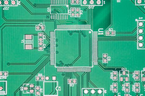
Moreover, the use of microvias is a defining characteristic of HDI PCBs.
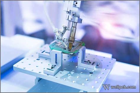
These are small-diameter vias that connect the different layers of the PCB. The materials used for microvias must be carefully selected to ensure reliability and performance. Typically, laser drilling is employed to create these microvias, and the choice of dielectric material is crucial to ensure clean and precise drilling. The filling of these microvias with conductive material, often copper, is another critical step that requires precision and high-quality materials.
In conclusion, the construction of HDI PCBs relies on a combination of advanced materials that work in concert to deliver superior performance and miniaturization. From high-performance substrates and conductive copper layers to advanced dielectrics and precise solder masks, each material plays a vital role in the overall functionality and reliability of the PCB. As technology continues to evolve, the development and refinement of these materials will remain at the forefront of HDI PCB manufacturing, driving further innovations in the electronics industry.
Advantages Of HDI PCBs In Modern Electronics
High-Density Interconnect (HDI) printed circuit boards (PCBs) have become a cornerstone in the advancement of modern electronics, offering a multitude of advantages that cater to the ever-evolving demands of technology. As electronic devices continue to shrink in size while increasing in functionality, the need for more efficient and compact circuit board designs has become paramount. HDI PCBs address this need by providing a solution that enhances performance, reliability, and design flexibility.
One of the primary advantages of HDI PCBs is their ability to support higher component density.
By utilizing finer lines and spaces, smaller vias, and capture pads, HDI technology allows for more components to be placed on both sides of the board. This increased density is crucial for modern electronic devices, such as smartphones, tablets, and wearable technology, where space is at a premium. Consequently, HDI PCBs enable manufacturers to design smaller, lighter, and more portable devices without compromising on functionality or performance.
In addition to supporting higher component density, HDI PCBs also offer improved electrical performance.
The shorter distances between components reduce signal loss and electromagnetic interference, which are common issues in traditional PCB designs. This results in faster signal transmission and improved overall performance of the electronic device. Furthermore, the use of microvias in HDI PCBs enhances signal integrity by minimizing the parasitic inductance and capacitance that can degrade signal quality. As a result, HDI PCBs are particularly well-suited for high-speed and high-frequency applications, such as advanced computing systems and telecommunications equipment.
Another significant advantage of HDI PCBs is their contribution to enhanced thermal management.
As electronic devices become more powerful, they generate more heat, which can adversely affect performance and reliability. HDI PCBs help mitigate this issue by providing better heat dissipation pathways. The use of thinner dielectric materials and the ability to incorporate thermal vias allow for more efficient heat transfer away from critical components. This improved thermal management not only enhances the longevity of the device but also ensures consistent performance under demanding conditions.
Moreover, HDI PCBs offer greater design flexibility, which is essential for the development of innovative electronic products.
The ability to incorporate multiple layers and blind or buried vias allows designers to create complex circuits that would be impossible with traditional PCB technology. This flexibility enables the integration of advanced features and functionalities, paving the way for cutting-edge applications in various industries, including automotive, aerospace, and medical devices.
In addition to these technical advantages, HDI PCBs also contribute to cost savings in the long run.
Although the initial manufacturing costs may be higher due to the complexity of the design and fabrication processes, the benefits of reduced size, weight, and improved performance often outweigh these costs. The ability to integrate more functions into a single board can lead to a reduction in the number of components required, thereby lowering assembly costs and improving overall product reliability.
In conclusion, the advantages of HDI PCBs in modern electronics are manifold, ranging from higher component density and improved electrical performance to enhanced thermal management and design flexibility. As the demand for more compact, efficient, and powerful electronic devices continues to grow, HDI technology will undoubtedly play a pivotal role in shaping the future of electronics, driving innovation and enabling the development of next-generation products.
Challenges And Solutions In HDI PCB Design
High-Density Interconnect (HDI) printed circuit boards (PCBs) have become a cornerstone in the advancement of modern electronics, offering enhanced performance and miniaturization. However, the design and construction of HDI PCBs present a unique set of challenges that require innovative solutions. As the demand for more compact and efficient electronic devices grows, engineers and designers must navigate these complexities to deliver reliable and high-performing products.
One of the primary challenges in HDI PCB design is managing the increased density of components and interconnections.
As devices become smaller, the need for more connections within a limited space becomes critical. This necessitates the use of finer lines and spaces, smaller vias, and more layers, which can complicate the manufacturing process. To address this, designers often employ advanced techniques such as laser drilling for microvias and sequential lamination processes. These methods allow for the creation of smaller and more precise features, enabling the accommodation of more components without compromising the board’s integrity.
Another significant challenge is signal integrity, which becomes increasingly difficult to maintain as the density of the PCB increases.
High-speed signals can suffer from issues such as crosstalk, electromagnetic interference (EMI), and signal attenuation. To mitigate these problems, designers must carefully consider the layout and routing of traces. Utilizing techniques such as controlled impedance routing, differential pair routing, and the strategic placement of ground planes can help preserve signal quality. Additionally, incorporating advanced simulation tools during the design phase can predict potential signal integrity issues, allowing for preemptive adjustments.
Thermal management is also a critical concern in HDI PCB design.
The compact nature of these boards can lead to significant heat accumulation, which can adversely affect performance and reliability. Effective thermal management strategies are essential to dissipate heat efficiently. Solutions such as the use of thermal vias, heat sinks, and thermal interface materials can help manage heat distribution. Moreover, selecting materials with high thermal conductivity for the PCB substrate can further enhance heat dissipation.
The complexity of HDI PCB design also extends to the manufacturing process, where precision and accuracy are paramount.
The use of advanced fabrication techniques, such as laser direct imaging and automated optical inspection, ensures that the intricate designs are accurately translated into physical boards. However, these advanced processes can increase production costs and time. To balance these factors, collaboration between designers and manufacturers is crucial. Early involvement of manufacturing experts in the design process can lead to more manufacturable designs, reducing the likelihood of costly revisions and delays.
Furthermore, the rapid pace of technological advancement necessitates continuous learning and adaptation.
Designers must stay abreast of the latest materials, tools, and techniques to remain competitive. Engaging in ongoing education and training, as well as participating in industry forums and conferences, can provide valuable insights and foster innovation.
In conclusion, while HDI PCB design presents several challenges, a combination of advanced techniques, careful planning, and collaboration can lead to successful outcomes. By addressing issues related to component density, signal integrity, thermal management, and manufacturing precision, designers can create high-performance PCBs that meet the demands of modern electronic devices. As technology continues to evolve, the ability to overcome these challenges will be essential in driving further advancements in the field.